Supercharge Your Innovation With Domain-Expert AI Agents!

Bidirectional electronic switch

a bidirectional electronic switch and switch technology, applied in the direction of diodes, semiconductor devices, electrical apparatus, etc., can solve the problems of high turn-on resistance and voltage, high manufacturing cost, and similar construction complexity, and achieve the effect of cheaper and easier fabrication, simple construction, and reduced manufacturing cos

Active Publication Date: 2011-07-19
SANKEN ELECTRIC CO LTD
View PDF11 Cites 12 Cited by
  • Summary
  • Abstract
  • Description
  • Claims
  • Application Information

AI Technical Summary

Benefits of technology

[0007]The present invention has it as an object to make the prior art bidirectional switching device, and particularly that of WO 2004 / 114508, simpler in construction, smaller in size, and cheaper and easier of fabrication than heretofore.
[0008]Another object of the invention is to stabilize the reference potential required for gating by the improved bidirectional switching device of the invention.
[0010]Electrically, the bidirectional switching device of the foregoing construction is equivalent to the prior art device according to WO 2004 / 114508 cited above. The two main electrodes and gate electrode provide in combination with the main semiconductor region a semiconductor switch (e.g., high electron mobility transistor or other device depending upon the specific configuration of the main semiconductor region). The two main electrodes and two diode-forming electrodes constitute two diodes in combination with the main semiconductor region. The semiconductor switch is in parallel with the two diodes which are in inverse series with each other. Thus, instead of being self-contained as in the prior art, the semiconductor switch and the diodes share the main electrodes. The bidirectional switching device according to the invention is therefore simpler in construction, smaller in size, and easier and less costly of manufacture.
[0011]A further reduction in size and manufacturing cost is realized as the two main electrodes serve both as the main electrodes (e.g., either source or drain of a HEMT) of the semiconductor switch and as the electrodes (e.g., cathodes) of the diodes. Additionally, the semiconductor switch and two diodes are themselves more compactly integrated than heretofore, contributing to a higher speed operation of the bidirectional switching device through curtailment of parasitic impedance.

Problems solved by technology

The TRIAC has the weakness that, once triggered, it cannot be turned off at a controllable point in an AC cycle; rather, it remains conductive until the current flowing therethrough drops below a predetermined threshold.
These prior art bidirectional switching circuits, all incorporating normally-off solid-state switches, are alike in being unnecessarily complex in construction and high in turn-on resistance and voltage.
Moreover, being made from semiconducting silicon materials with relatively low bandgaps, such known devices are not so high in antivoltage strength as can be desired.
Offsetting these benefits are its bulkiness and high manufacturing costs resulting from use of some unnecessarily self-contained components that are essential for its functioning.
Difficulties have also been experienced in providing a reference potential needed for gating.

Method used


Image

  • Bidirectional electronic switch
  • Bidirectional electronic switch
  • Bidirectional electronic switch

Examples


embodiment

of FIG. 7

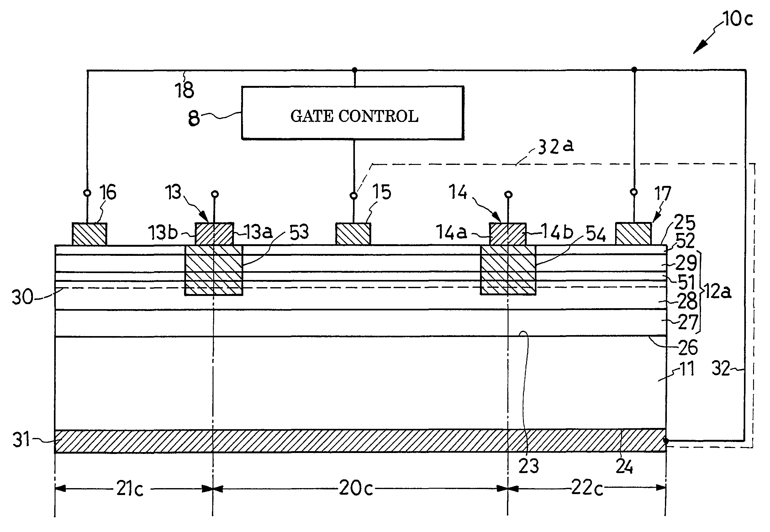
[0078]The semiconductor switch 20b and diodes 21b and 22b of this bidirectional switching device 10b are similar to their FIG. 5 counterparts 20a, 21a and 22a in having the substrate electrode 31 on the back 24 of the silicon substrate 11a. The substrate electrode 31 is electrically connected to the gate electrode 15 via the gate control circuit 8 but, unlike the preceding embodiments, not directly to the diode-forming electrodes 16 and 17. This embodiment features the following means 18a for electrically interconnecting the two diode-forming electrodes 16 and 17 but is otherwise identical with that of FIG. 3.

[0079]The first diode-forming electrode 16 is electrically coupled to the electroconductive substrate 11a via a conductor 41 and bonding pad 42, the latter being formed on a ledge 23 of the substrate. The second diode-forming electrode 17 is electrically coupled to the substrate 11a via another conductor 43 and another bonding pad 44 on another ledge of the substrate. ...


PUM


Abstract

A main semiconductor region grown on a substrate has formed on its surface a pair of main electrodes spaced from each other, a gate electrode between the main electrodes, and a pair of diode-forming electrodes spaced farther away from the gate electrode than are the main electrodes. Making ohmic contact with the main semiconductor region, the pair of main electrodes serve both as drain or source of a HEMT switch and as cathodes of a pair of Schottky diodes integrated with the HEMT switch. Both gate electrode and diode-forming electrodes are in Schottky contact with the main semiconductor region.

Description

CROSS REFERENCE TO RELATED APPLICATIONS[0001]This application claims priority to Japanese Patent Application No. 2007-330690, filed Dec. 21, 2007.BACKGROUND OF THE INVENTION[0002]This invention relates generally to switches, to electronic switches, and particularly to bidirectional, or alternating current (AC), switches for use in or with a variety of electric circuits notably including matrix converters and AC power supplies.[0003]Perhaps the most familiar example of AC switches is a bidirectional triode thyristor, better known as TRIAC (TRIode for Alternating Current). The TRIAC has the weakness that, once triggered, it cannot be turned off at a controllable point in an AC cycle; rather, it remains conductive until the current flowing therethrough drops below a predetermined threshold.[0004]Some bidirectional switching devices have been known which meet that requirement. One of them (shown in FIG. 1 of the drawings attached hereto) comprises two insulated-gate bipolar transistors ...

Claims


Application Information

Patent Timeline
Patent Type & Authority Patents(United States)
IPC IPC(8): H01L29/872H01L29/66
CPCH01L27/0605H01L27/0629H01L29/7783H01L29/7787H01L29/872H01L29/2003
Inventor MACHIDA, OSAMU
Owner SANKEN ELECTRIC CO LTD
Features
  • R&D
  • Intellectual Property
  • Life Sciences
  • Materials
  • Tech Scout
  • Unparalleled Data Quality
  • Higher Quality Content
  • 60% Fewer Hallucinations
Learn More