Variable resistance memory device having reduced bottom contact area and method of forming the same

a memory device and variable resistance technology, applied in the field of variable resistance memory elements, can solve the problem that the conventional variable resistance memory elements require large operating currents

Active Publication Date: 2011-08-02
MICRON TECH INC
View PDF4 Cites 12 Cited by
  • Summary
  • Abstract
  • Description
  • Claims
  • Application Information

AI Technical Summary

Problems solved by technology

Often, however, conventional variable resistance memory elements require large operating currents.

Method used


Image

  • Variable resistance memory device having reduced bottom contact area and method of forming the same
  • Variable resistance memory device having reduced bottom contact area and method of forming the same
  • Variable resistance memory device having reduced bottom contact area and method of forming the same

Examples


Embodiment Construction

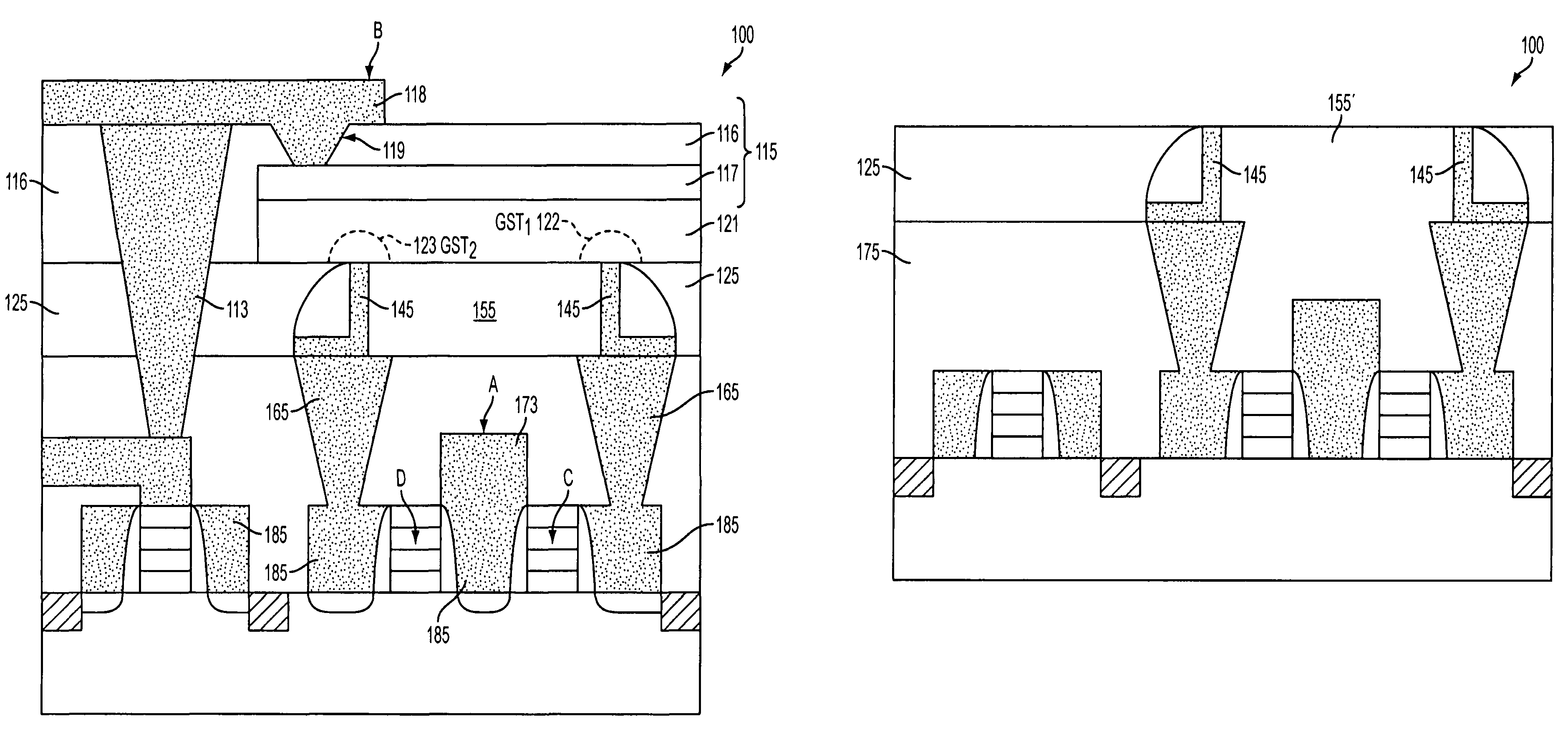
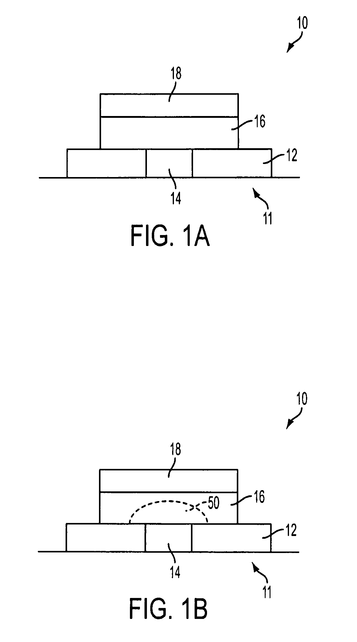
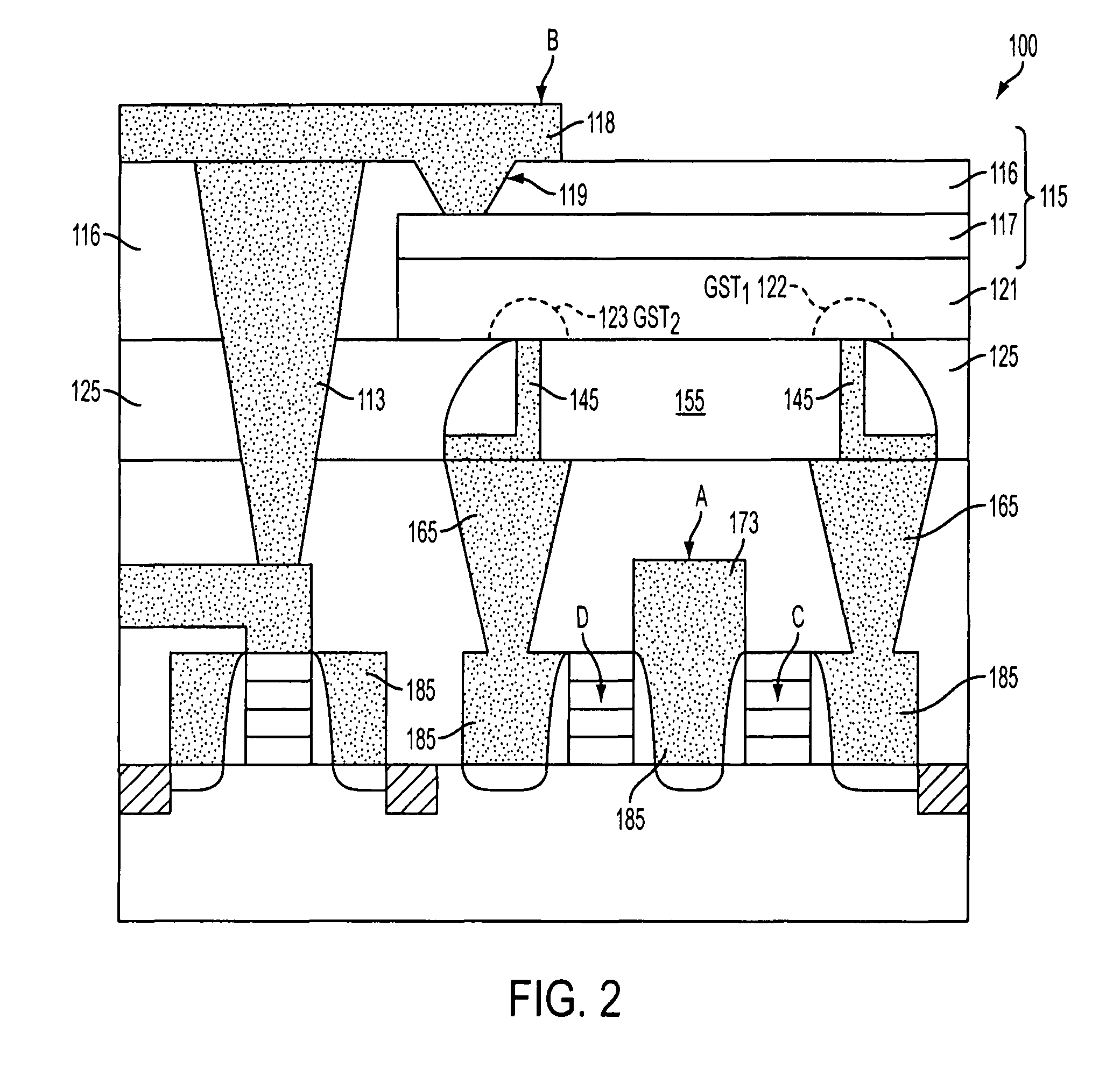
[0025]In the following detailed description, reference is made to various specific embodiments. These embodiments are described with sufficient detail to enable those skilled in the art to practice the claimed invention. It is to be understood that other embodiments may be employed, and that various structural, logical and electrical changes may be made.

[0026]The term “substrate” used in the following description may include any supporting structure including, but not limited to, a semiconductor substrate that has an exposed substrate surface. A semiconductor substrate should be understood to include silicon, silicon-on-insulator (SOI), silicon-on-sapphire (SOS), doped and undoped semiconductors, epitaxial layers of silicon supported by a base semiconductor foundation, and other semiconductor structures, including those made of semiconductors other than silicon. When reference is made to a semiconductor substrate or wafer in the following description, previous process steps may have...


PUM


Abstract

A variable resistance memory element and method of forming the same. The memory element includes a substrate supporting a bottom electrode having a small bottom contact area. A variable resistance material is formed over the bottom electrodes such that the variable resistance material has a surface that is in electrical communication with the bottom electrode and a top electrode is formed over the variable resistance material. The small bottom electrode contact area reduces the reset current requirement which in turn reduces the write transistor size for each bit.

Description

FIELD OF THE INVENTION[0001]Embodiments of the invention relate to semiconductor devices, and in particular to variable resistance memory elements and methods of forming and using the same.BACKGROUND OF THE INVENTION[0002]Non-volatile memories are important elements of integrated circuits due to their ability to maintain data absent a power supply. Several different typical resistance memory elements using different materials have been suggested for such use. Variable resistance memory elements can be programmed to a resistance value as a way of storing logic data. One suggested type of resistance memory employs phase change materials such as chalcogenide alloys, which are capable of stably transitioning between amorphous and crystalline phases. Each phase exhibits a particular resistance state and the resistance states distinguish the logic values of the memory element. Specifically, an amorphous state exhibits a relatively high resistance, and a crystalline state exhibits a relati...

Claims


Application Information

Patent Timeline
Patent Type & Authority Patents(United States)
IPC IPC(8): H01L21/00
CPCH01L45/06H01L45/1233H01L45/1273H01L27/2472H01L45/16H01L27/2436H01L45/144H10B63/30H10B63/82H10N70/231H10N70/826H10N70/8418H10N70/8828H10N70/011
Inventor NEJAD, HASAN
Owner MICRON TECH INC
Why Eureka
Try Eureka