Semiconductor device packages with electromagnetic interference shielding

a technology of electromagnetic interference shielding and semiconductor devices, which is applied in the field of semiconductor device packages with electromagnetic interference shielding, can solve the problems of reducing the level of emissions that can pass through the casing, adversely affecting neighboring semiconductor devices, and progressively more complex semiconductor devices

Active Publication Date: 2011-08-02
ADVANCED SEMICON ENG INC
View PDF165 Cites 108 Cited by
  • Summary
  • Abstract
  • Description
  • Claims
  • Application Information

AI Technical Summary

Benefits of technology

[0009]Another aspect of the invention relates to methods of forming semiconductor device packages with EMI shielding. In one embodiment, a method includes, (1) providing a substrate including (a) an upper surface, (b) a lower surface, and (c) grounding vias partially extending between the upper surface and the lower surface of the substrate, such that a height of each of the grounding vias is less than a thickness of the substrate; (2) electrically connecting a semiconductor device to the upper surface of the substrate; (3) applying a molding material to the upper surface of the substrate to form a molded structure covering the semiconductor device; (4) forming cutting slits

Problems solved by technology

Semiconductor devices have become progressively more complex, driven at least in part by the demand for enhanced processing speeds and smaller sizes.
While the benefits of enhanced processing speeds and smaller sizes are apparent these characteristics of semiconductor devices also can create problems.
If the level of electromagnetic emissions at a neighboring semiconductor device is sufficiently high, these emissions can adversely affect the operation of that semiconductor device.
When electromagnetic emissions from an interior of the package strike an inner surface of the casing, at least a portion of these emissions can be electrically shorted, thereby reducing the level of emissions that can pass through the casing and adversely affect neighboring semi

Method used


Image

  • Semiconductor device packages with electromagnetic interference shielding
  • Semiconductor device packages with electromagnetic interference shielding
  • Semiconductor device packages with electromagnetic interference shielding

Examples


Embodiment Construction

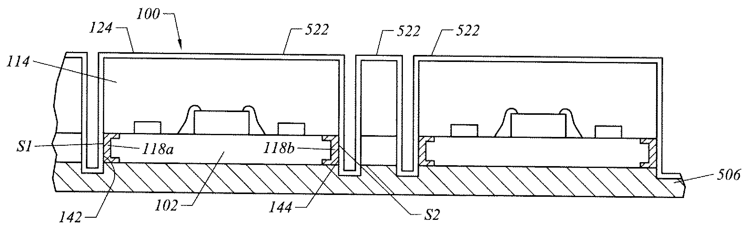
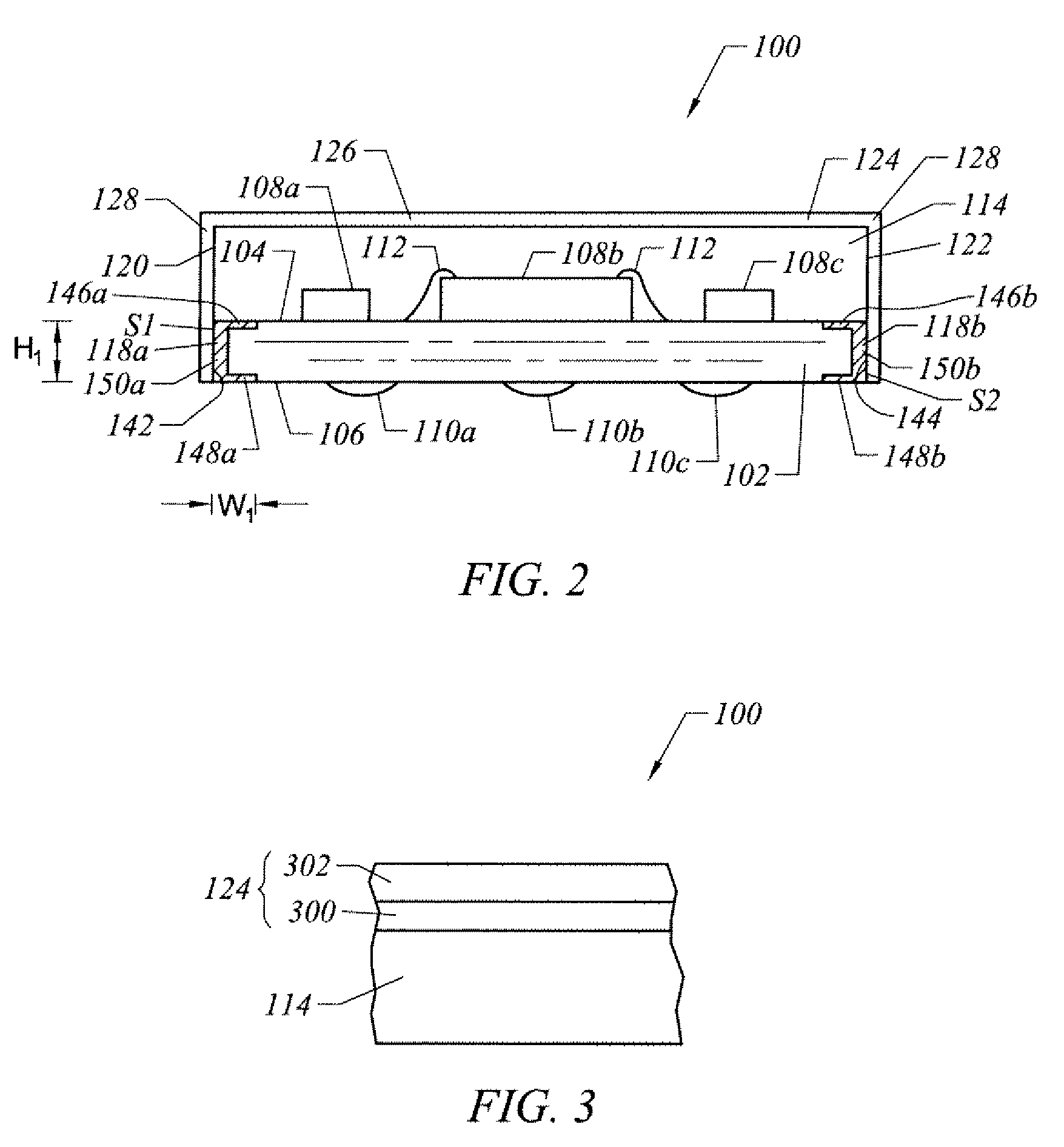
emiconductor device package of FIG. 1.

[0015]FIG. 4A illustrates a cross-sectional view of a semiconductor device package implemented in accordance with another embodiment of the invention.

[0016]FIG. 4B illustrates a cross-sectional view of a semiconductor device package implemented in accordance with another embodiment of the invention.

[0017]FIG. 4C illustrates a cross-sectional view of a semiconductor device package implemented in accordance with another embodiment of the invention.

[0018]FIG. 5A through FIG. 5E illustrate a method of forming the semiconductor device package of FIG. 1, according to an embodiment of the invention.

[0019]FIG. 6 illustrates a method of forming the semiconductor device package of FIG. 4A, according to another embodiment of the invention.

DETAILED DESCRIPTION

Definitions

[0020]The following definitions apply to some of the aspects described with respect to some embodiments of the invention. These definitions may likewise be expanded upon herein.

[0021]As used...


PUM

PropertyMeasurementUnit
Widthaaaaaaaaaa
Widthaaaaaaaaaa
Heightaaaaaaaaaa

Abstract

Described herein are semiconductor device packages with EMI shielding and related methods. In one embodiment, a semiconductor device package includes: (1) a substrate unit including a grounding element; (2) a semiconductor device disposed adjacent to an upper surface of the substrate unit; (3) a package body disposed adjacent to the upper surface of the substrate unit and covering the semiconductor device; and (4) an EMI shield disposed adjacent to exterior surfaces of the package body and electrically connected to a connection surface of the grounding element. A lateral surface of the package body is substantially aligned with a lateral surface of the substrate unit, and the connection surface of the grounding element is electrically exposed adjacent to the lateral surface of the substrate unit. The grounding element corresponds to a remnant of an internal grounding via, and provides an electrical pathway to ground electromagnetic emissions incident upon the EMI shield.

Description

CROSS REFERENCE TO RELATED APPLICATIONS[0001]This application is a continuation-in-part of U.S. patent application Ser. No. 12 / 336,400, filed on Dec. 16, 2008, which claims the benefit of U.S. Provisional Application Ser. No. 61 / 006,894, filed on Feb. 5, 2008, and the benefit of Taiwan Application Serial No. 97115985, filed on Apr. 30, 2008, the disclosures of which are incorporated herein by reference in their entireties.FIELD OF THE INVENTION[0002]The invention relates generally to semiconductor device packages. More particularly, the invention relates to semiconductor device packages with electromagnetic interference shielding.BACKGROUND[0003]Semiconductor devices have become progressively more complex, driven at least in part by the demand for enhanced processing speeds and smaller sizes. While the benefits of enhanced processing speeds and smaller sizes are apparent these characteristics of semiconductor devices also can create problems. In particular, higher clock speeds can i...

Claims


Application Information

Patent Timeline
IPC IPC(8): H01L23/552H01L21/56
CPCH01L23/3121H01L24/97H01L21/568H01L21/6835H01L23/49805H01L23/552H01L2924/01002H01L2924/01033H01L2924/19043H01L2224/48227H01L2224/97H01L2924/01005Y10T29/49165H01L2224/49175Y10T29/49146H01L2924/19042H01L2924/01047H01L2221/68345H01L2924/3025H01L2924/19041H01L2924/01027H01L2924/01075H01L2924/01006H01L2924/19105H01L2924/15311H01L2924/01024H01L24/48H01L2924/01013H01L2924/01078Y10T29/49153H01L2924/01029H01L2224/48091H01L2924/01082H01L2924/01079H01L2924/16152H01L2224/16225H01L2924/014Y10T29/49789H01L2924/00014H01L2224/85H01L2224/81H01L2224/81005H01L2224/85005H01L2924/181H01L24/49H01L2924/00H01L2924/00012H01L2224/45099H01L2224/45015H01L2924/207
Inventor LIAO, KUO-HSIENCHIU, CHI-TSUNGHUNG, CHIH-PIN
Owner ADVANCED SEMICON ENG INC
Why Eureka
Try Eureka