Method of manufacturing a patterned conductive layer

a technology of conductive layer and manufacturing method, which is applied in the direction of printed circuit dielectrics, transparent dielectrics, printed circuit aspects, etc., can solve the problems of not environmentally safe, high cost of etching process, and inability to meet fine patterns,

Inactive Publication Date: 2011-08-09
HANITA COATINGS R C A
View PDF20 Cites 6 Cited by
  • Summary
  • Abstract
  • Description
  • Claims
  • Application Information

AI Technical Summary

Problems solved by technology

As the thickness of a standard copper film is between 18 microns and 35 microns and the thickness required for a typical antenna or a typical electrode is 11-15 microns, the etching process becomes very expensive and slow in addition to being not environmentally safe.
The printing process is expensive and not suitable for fine patterns.
The low electrical conductivity of standard conductive inks is another drawback of this process.
TCE's may be also produced by lamination of a metallic mesh to a substrate in a rather expensive and complicated process.

Method used


Image

  • Method of manufacturing a patterned conductive layer
  • Method of manufacturing a patterned conductive layer
  • Method of manufacturing a patterned conductive layer

Examples


Embodiment Construction

[0007]In the following detailed description, numerous specific details are set forth in order to provide a thorough understanding of the invention. However it will be understood by those of ordinary skill in the art that the embodiments of present invention may be practiced without these specific details. In other instances, well-known methods, procedures and components have not been described in detail so as not to obscure the present invention.

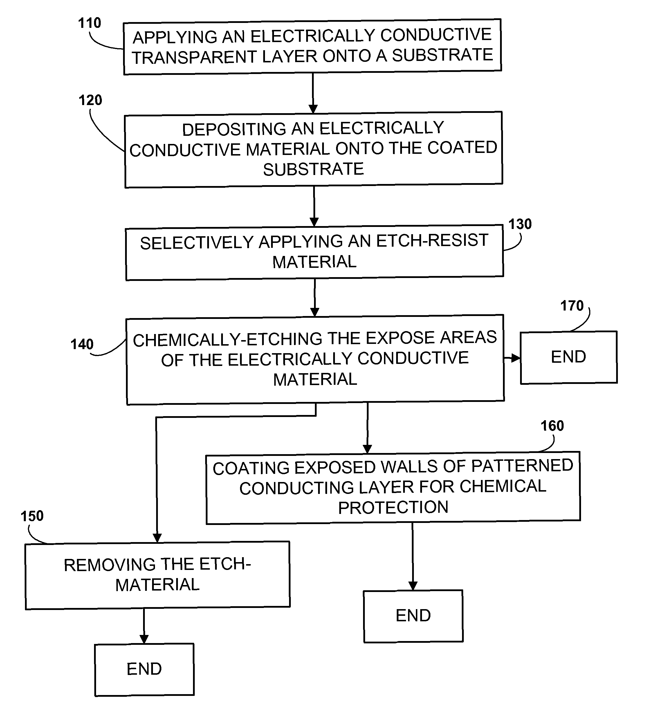
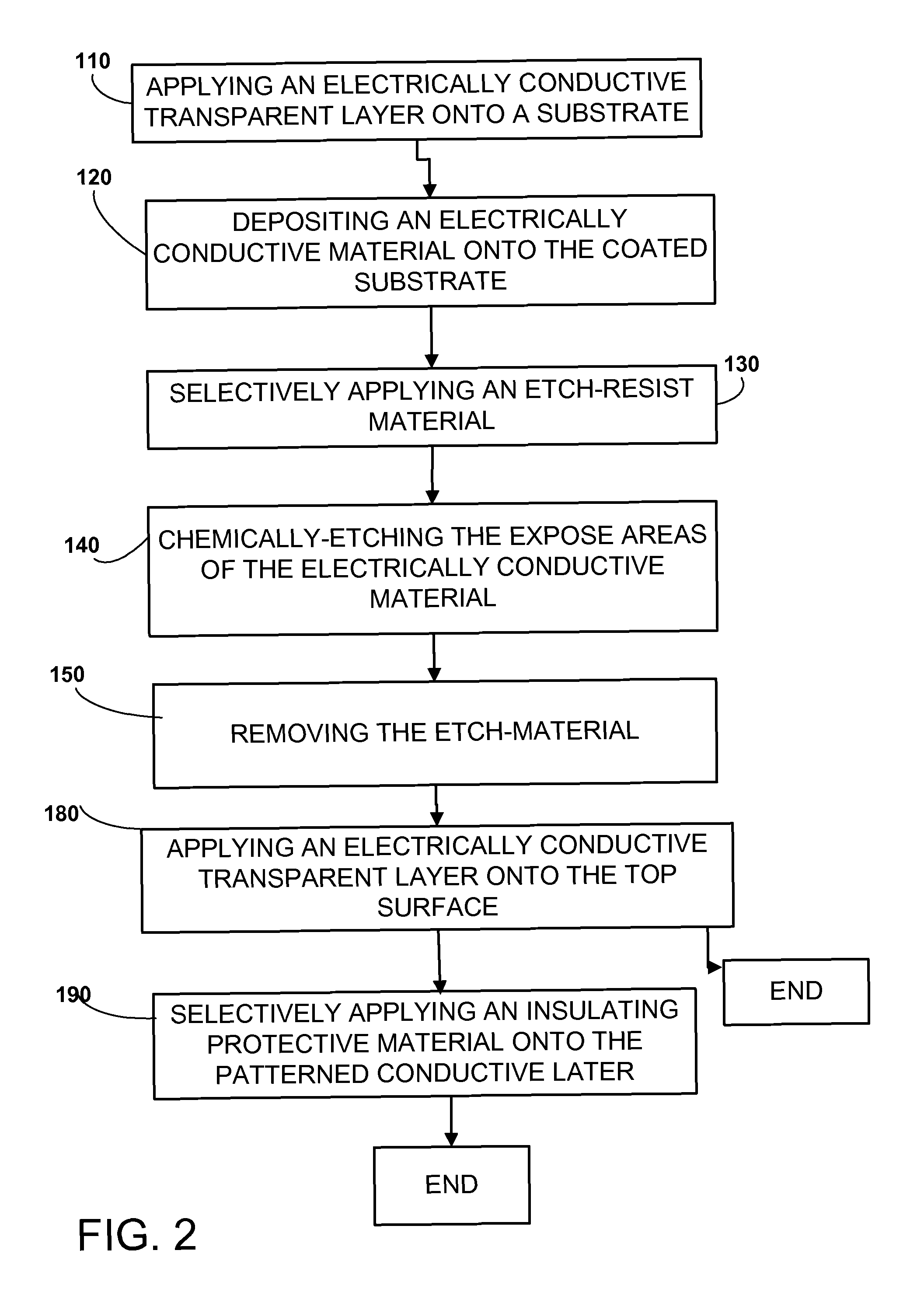
[0008]Embodiments of the present invention are directed to a method of producing a pattern of electrically conductive objects on a substrate. According to some embodiments of the present invention, the conductive objects may be flexible circuits. According to other embodiments of the present invention, the conductive objects may be metallic grids (mesh) useful for example as transparent conductive electrodes (TCEs) or heaters.

[0009]According to some embodiments of the invention, the method may include applying onto a substrate a coating laye...


PUM

PropertyMeasurementUnit
thicknessaaaaaaaaaa
thicknessaaaaaaaaaa
thicknessaaaaaaaaaa

Abstract

According to embodiments of the present invention, a method for manufacturing a pattern of conductive elements on a substrate is provided. The method includes applying a coating layer of electrically conductive transparent compounds onto a substrate; depositing in a vacuum deposition chamber an electrically conductive material onto the coating layer to form an electrically conductive layer; applying an etch-resist material on selective areas of the electrically conductive layer, wherein the selective areas are substantially areas pre-designed to carry the conductive objects; and chemically etching the electrically conductive material from exposed areas of the electrically conductive layer that are not covered by the etch-resist material.

Description

CROSS REFERENCE TO RELATED APPLICATIONS[0001]The present application is a continuation-in-part application of patent application Ser. No. 11 / 730,424, filed Apr. 2, 2007 now U.S. Pat. No. 7,578,048, which claims benefit of U.S. Provisional Patent application Ser. No. 60 / 788,728, filed Apr. 4, 2006, both of which are incorporated by reference in their entirety.BACKGROUND OF THE INVENTION[0002]Many industrial applications involve laying down patterns of conductive material on a substrate to produce devices and flexible electronic circuits like, for example, bus bars and shunting lines for flat displays and lighting devices and transparent conductive electrodes (TCEs) for solar cells. A transparent conductive electrode, which may include a patterned grid of conductive material, enables transmission of visible light trough the grid. The average light transmission ratio may vary between 0.2% and 99.9% and for most cases enables substantial visibility through the grid. A conventional metho...

Claims


Application Information

Patent Timeline
Patent Type & Authority Patents(United States)
IPC IPC(8): H05K3/30
CPCH01P11/003H05B3/84H05K3/24H05K9/0096H01Q1/38Y10T29/49124H05B2203/017H05K1/0393H05K3/061H05K3/243H05K2201/0108H05K2201/0326H05K2201/0329H05K2203/0315H05K2203/0571Y10T29/49155Y10T29/49117Y10T29/4913Y10T29/49002Y10T29/49156
Inventor CARMI, YOASH
Owner HANITA COATINGS R C A
Why Eureka
Try Eureka