Illumination system for a microlithographic projection exposure apparatus

a technology of exposure apparatus and exposure device, which is applied in the direction of microlithography exposure apparatus, printers, instruments, etc., can solve the problems of difficult preservation of the polarization state of illumination light with such light mixing elements, and the inability to change the geometrical optical flux by conventional refractive optical elements such as lenses, and achieve the effect of enhancing the irradiance uniformity in the reticle plane, compact and easy construction

Inactive Publication Date: 2011-08-23
CARL ZEISS AG
View PDF40 Cites 7 Cited by
  • Summary
  • Abstract
  • Description
  • Claims
  • Application Information

AI Technical Summary

Benefits of technology

[0023]By providing two different optical raster elements it is possible to increase the geometrical optical flux independently for two perpendicular directions. This is advantageous because usually the illuminated field on a reticle has a rectangular geometry in which the short sides of the rectangle are aligned parallel to the scan direction. As a result, the increase of the geometrical optical flux required for the scan direction is smaller than in the direction perpendicular thereto. This allows to optimize two or more optical raster elements for their respective task, i.e. to generate a desired intensity distribution in one direction. The better the far field intensity distribution generated by the raster elements is adapted to the desired geometry of the illuminated field, the less are light losses incurred by field stops.
[0043]According to another aspect of the invention, an illumination system for a microlithographic projection exposure apparatus comprises a light source and a scattering arrangement producing a scattering effect that varies during exposures. This avoids undesired interactions between scattering structures contained in the scattering arrangement on the one hand and regular features contained in a field defining element. Such interactions may otherwise cause irradiance fluctuations in the mask plane.

Problems solved by technology

Since the geometrical optical flux is not altered when a light bundle traverses an interface between media having different refractive indices, the geometrical optical flux cannot be changed by conventional refractive optical elements such as lenses.
However, it is difficult to preserve the polarization state of the illumination light with such light mixing elements.
This is disadvantageous because it has been found out that illuminating the reticle with illumination light having a carefully selected polarization state may considerably improve the imaging of the reticle onto the photoresist.
However, is has been found out that using such a stop device alone does not meet the required accuracy with respect to the irradiance uniformity.
Diffractive optical elements have the disadvantage that the zero's diffraction order cannot be sufficiently suppressed.
This significantly reduces the diffraction efficiency of the device to values below 80%.
In addition, the manufacture by electron beam lithography is a very slowly process so that these elements are extremely expensive.
The main drawback of refractive optical elements, however, is the fact that the intensity distribution generated in the far field and thus in the reticle plane is not sufficiently uniform.

Method used


Image

  • Illumination system for a microlithographic projection exposure apparatus
  • Illumination system for a microlithographic projection exposure apparatus
  • Illumination system for a microlithographic projection exposure apparatus

Examples


Embodiment Construction

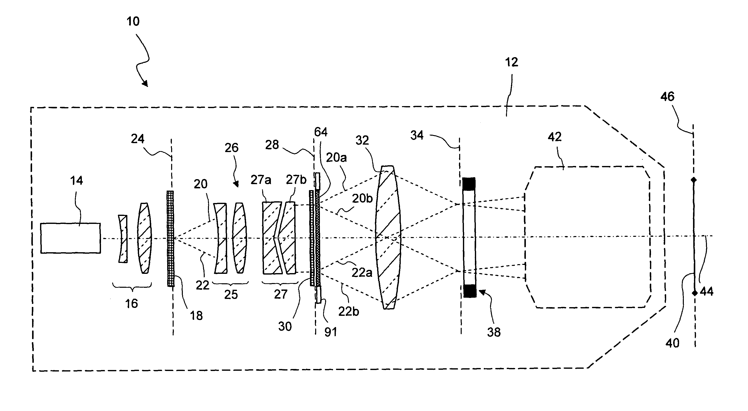
[0070]FIG. 1 shows a meridional section of an illumination system according to the present invention that is to be used in a projection exposure step-and-scan apparatus. For the sake of clarity, the illustration shown in FIG. 1 is considerably simplified and not to scale. The illumination system, which is denoted in its entirety by 10, comprises a light source that is, in the embodiment shown, realized as an excimer laser 14. The excimer laser 14 emits illumination light that has a wavelength in the deep ultraviolet (DUV) spectral range, for example 193 nm. The illumination light emerging from the exit facet of the laser 14 forms a partially coherent light bundle having a small cross section and a low divergence. Thus the geometrical optical flux of the light bundle as emitted by the laser 14 is small.

[0071]The light bundle then enters a beam expansion unit 16 in which the light bundle is expanded. Since the light bundle is diverted at refractive interfaces, the cross section of the...


PUM

PropertyMeasurementUnit
anglesaaaaaaaaaa
distanceaaaaaaaaaa
distanceaaaaaaaaaa

Abstract

An illumination system for a microlithographic projection exposure step-and-scan apparatus has a light source, a first optical raster element and a second optical raster element. The first optical raster element extends in a first pupil plane of the illumination system and is designed such that the geometrical optical flux of the system is increased perpendicular to a scan direction of the projection exposure apparatus. The second optical raster element extends in a second pupil plane of the illumination system, which is not necessarily different from the first pupil plane, and is designed such that the geometrical optical flux of the system is increased in the scan direction and perpendicular thereto. This makes it possible to improve the irradiance uniformity in a reticle plane.

Description

CROSS-REFERENCE TO RELATED APPLICATIONS[0001]This is a continuation-in-part of international application PCT / EP2005 / 001501 filed Feb. 15, 2005 and claiming benefit of U.S. provisional application 60 / 545,105, which was filed Feb. 17, 2004. The full disclosure of these earlier applications is incorporated herein by reference.BACKGROUND OF THE INVENTION[0002]1. Field of the Invention[0003]The invention relates generally to illumination systems for microlithographic projection exposure apparatus. More particularly, the invention relates to illumination systems comprising an optical field defining component that is positioned in or in close proximity to a pupil plane of the illumination system. Such a field defining component determines, together with stops, the geometry and the intensity distribution of a field that is illuminated by the illumination system on a reticle to be projected.[0004]2. Description of Related Art[0005]Microlithography (also called photolithography) is a technolo...

Claims


Application Information

Patent Timeline
Patent Type & Authority Patents(United States)
IPC IPC(8): G03B27/54G03B27/52G03B27/72G03B27/42G03F7/20
CPCG03B27/54G03F7/7015G03F7/70108G03F7/70075G03F7/20G03F7/00
Inventor FIOLKA, DAMIANMAUL, MANFREDDAVYDENKO, VLADIMIRSCHOLZ, AXELDEGUENTHER, MARKUSWANGLER, JOHANNES
Owner CARL ZEISS AG
Why Eureka
Try Eureka