
Optically controlled electrical switching device based on wide bandgap semiconductors

a technology of wide bandgap semiconductors and switching devices, applied in electronic switching, pulse techniques, nanoinformatics, etc., can solve the problems of only being able to achieve substantial improvements, material quality and application markets have not been sufficiently mature until recently to justify significant manufacturing activities, and achieve greater power control efficiency. , the effect of high temperature operation

Inactive Publication Date: 2011-09-06
PETTIT JOHN W
View PDF14 Cites 4 Cited by
  • Summary
  • Abstract
  • Description
  • Claims
  • Application Information

AI Technical Summary

Benefits of technology

[0021]It is still another object of the invention to provide, at least in some embodiments, an optically controlled power switch that can operate at high temperatures and harsh environments useful for aerospace, defense and similar hostile environments.
[0046]Operation with wide bandgap semiconductors to achieve high temperature operation and the enhanced efficiencies of wide bandgap semiconductors in a light controlled mode of operation.

Problems solved by technology

Power switching devices are reaching fundamental limits imposed by the low breakdown field of silicon, and substantial improvements can only be achieved by going to semiconductors with a higher breakdown field.
While the inherent properties of these materials give them dramatic performance advantages over conventional semiconductors (e.g., Si and GaAs), the materials' quality and application markets have not been sufficiently mature until recently to justify significant manufacturing activities.
However, because of technological differences, power devices in SiC will be very different from silicon devices, and a direct translation of silicon concepts to SiC is not always possible.
However, these III-V nitride compounds do not possess a native oxide similar to SiO2, so true MOS devices will not be feasible.
In addition, the nitrides suffer from the lack of a suitable lattice-matched substrate for crystal growth, and hence the material is in a more primitive state of development than SiC.
Currently available optically controlled power switches in addition to being based on silicon and not offering the advantages of wide bandgap semiconductors, require an extremely large optical input signal to operate the device.
This places an immense burden on the optical fiber that carries the light to the device and the optical power source that generates the required light.
These factors add cost, complexity, and added waste heat generation to the system, which runs counter to the purpose of using these devices.
Light of a wavelength necessary to activate wide bandgap semiconductors falls into the ultraviolet region of the electromagnetic spectrum, and light of this wavelength is not very good for fiber optic operation.
Optical fibers simply do not transmit light at this wavelength very efficiently, and optical networks utilizing light at these wavelengths are not desired by the Air Force and the aerospace industry.
However, a working device according to that patent would require more power than is desired in the art to be used.
However, the art does not teach a way to combine the advantages of wide-bandgap semiconductors and carbon nanotubes or even the desirability of doing so.

Method used


Image

  • Optically controlled electrical switching device based on wide bandgap semiconductors
  • Optically controlled electrical switching device based on wide bandgap semiconductors
  • Optically controlled electrical switching device based on wide bandgap semiconductors

Examples


Embodiment Construction

[0055]A preferred embodiment will be set forth in detail with respect to the drawings, in which like reference numerals refer to like elements throughout.

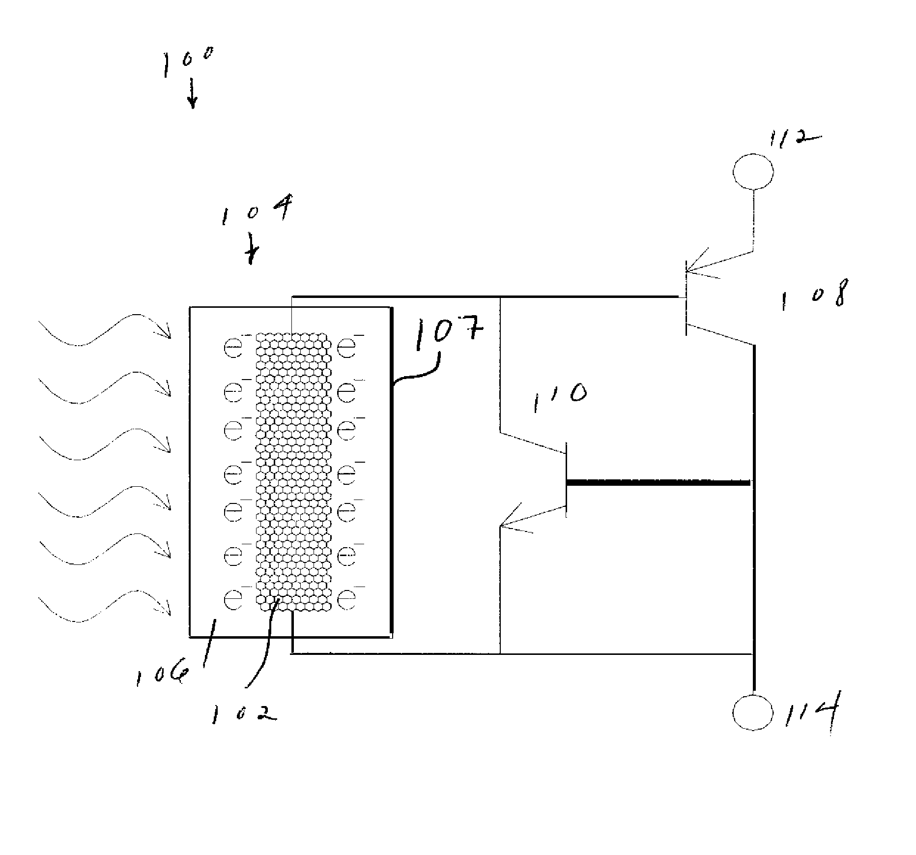
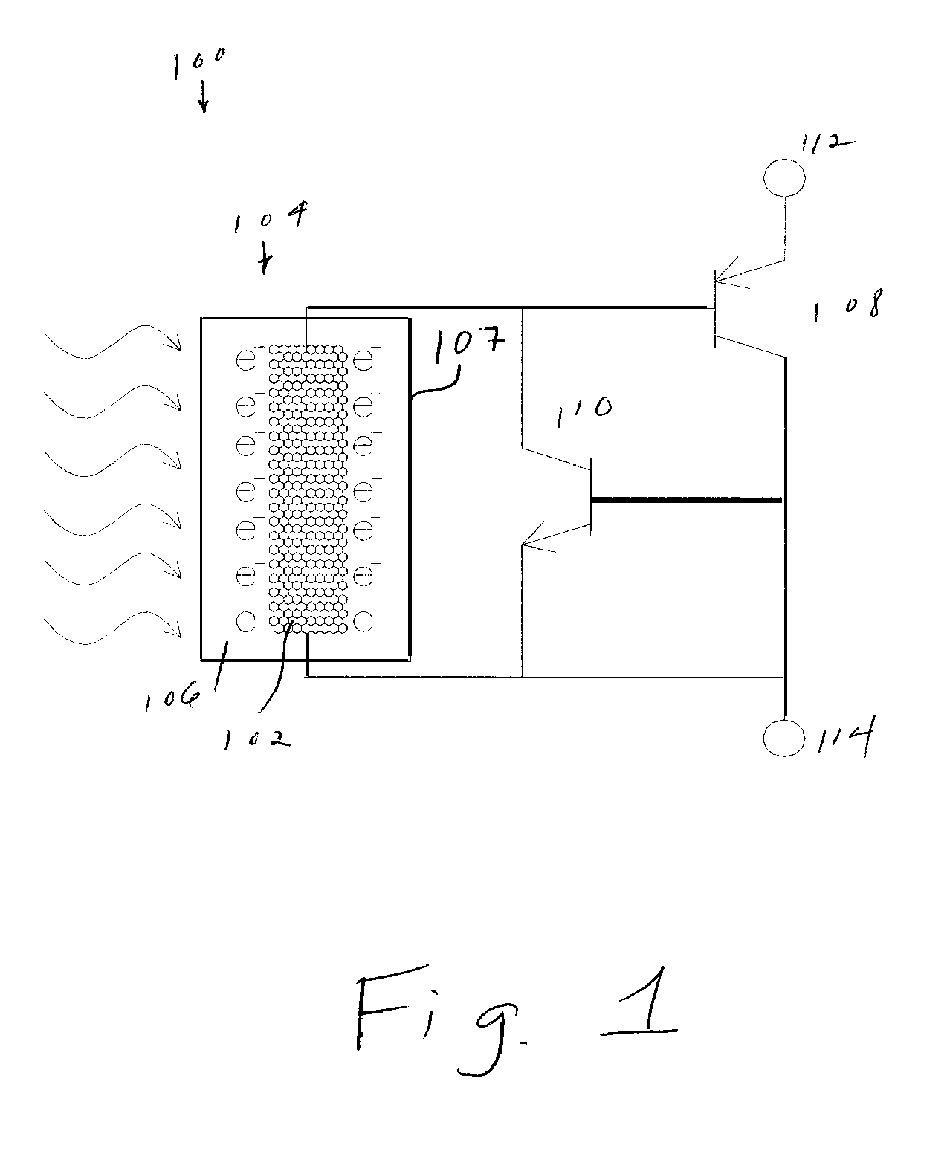
[0056]FIG. 1 shows a preferred embodiment of the switching device as 100. One or more semiconducting carbon nanotubes 102 form an optically gated FET 104 that in turn gates or switches on a power switching device. The power switching device has the topology of an SCR or IGBT, although other topologies can be implemented. The carbon nanotube FET 104 takes the place of the MOS FET in a customary IGBT arrangement. The carbon nanotube FET 104 is optically activated by light that is supplied by an optical fiber or any such optical means that creates charge near the nanotube surface when the light interacts with the photo-generating material 106, which can include a semiconductor substrate 107 on which the carbon nanotube 102 is disposed, surrounding the carbon nanotube 102. This charge acting on the carbon nanotube surface is denoted by...


PUM


Abstract

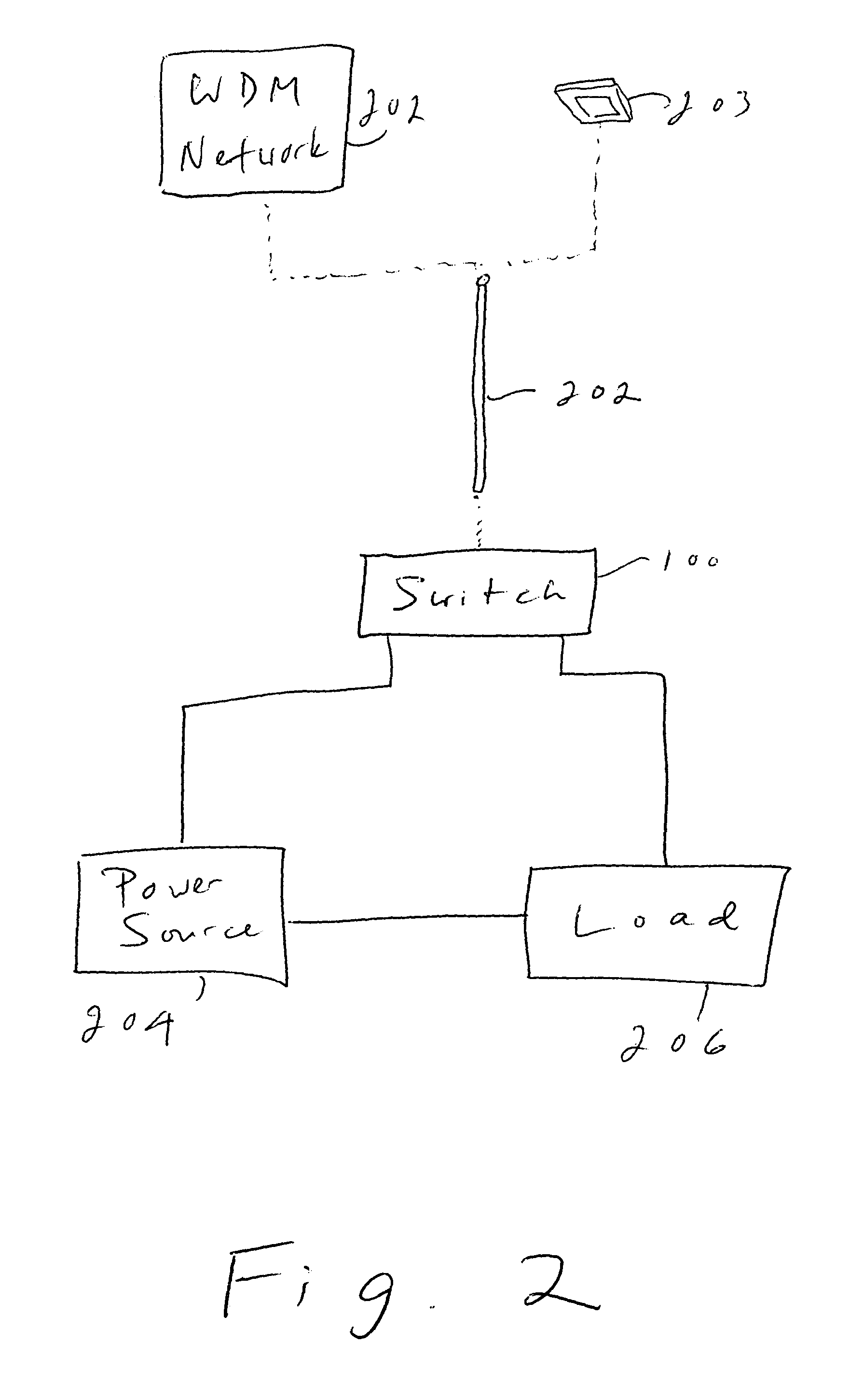
A power switching device includes an optically controlled component using a semiconducting carbon nanotube. An optical signal transmitted over an optical fiber controls the conductivity of the nanotube. The nanotube transmits a signal controlled by the optical signal to a wide-bandgap semiconductor power switch, which switches the power.

Description

REFERENCE TO RELATED APPLICATION[0001]The present application claims the benefit of U.S. Provisional Patent Application No. 60 / 533,151, filed Dec. 31, 2003, whose disclosure is hereby incorporated by reference into the present disclosure.FIELD OF THE INVENTION[0002]The present invention is directed to an optically controlled switching device and more particularly to such a device which exploits the advantages of wide bandgap (WBG) semiconductors.DESCRIPTION OF RELATED ART[0003]Power switching devices are reaching fundamental limits imposed by the low breakdown field of silicon, and substantial improvements can only be achieved by going to semiconductors with a higher breakdown field. Wide bandgap semiconductors, such as silicon carbide, SiC, have a bandgap of around 3 eV and 8 times the breakdown voltage and 100-200 times the on state conductivity of silicon. SiC can work at temperatures of 600 degrees Centigrade, has much better thermal conductivity than silicon, has a coefficient ...

Claims


Application Information

Patent Timeline
Patent Type & Authority Patents(United States)
IPC IPC(8): H01L31/111H01L31/10H01L31/11H01L51/00H01L51/42H03K17/78H03K17/795
CPCB82Y10/00B82Y20/00B82Y30/00H01L31/10H01L31/11H01L51/0504H03K17/78H03K17/795H01L2924/0002H01L51/0048H01L51/422H01L51/4253H01L51/428H01L2924/00H10K85/221H10K10/00H10K30/15H10K30/65H10K30/30
Inventor PETTIT, JOHN W.
Owner PETTIT JOHN W
Learn More