Multi-layered printed circuit board with a conductive substrate and three insulating layers with wiring and ground traces
a printed circuit board and substrate technology, applied in the field of printed circuit boards, can solve problems such as transmission errors, and achieve the effect of sufficiently preventing transmission errors
- Summary
- Abstract
- Description
- Claims
- Application Information
AI Technical Summary
Benefits of technology
Problems solved by technology
Method used
Image
Examples
first embodiment
[0052](1-1) Configuration of the Suspension Board
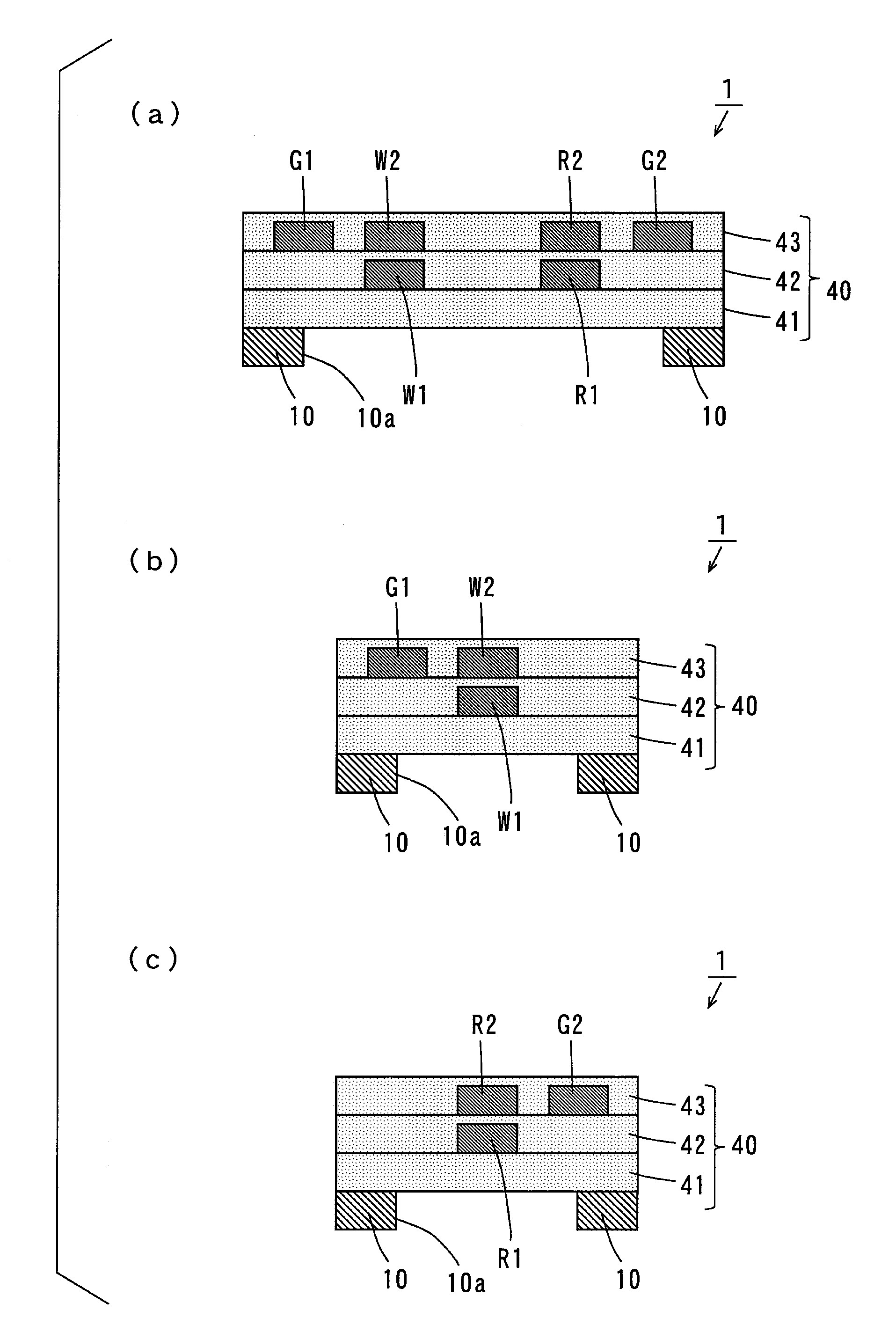
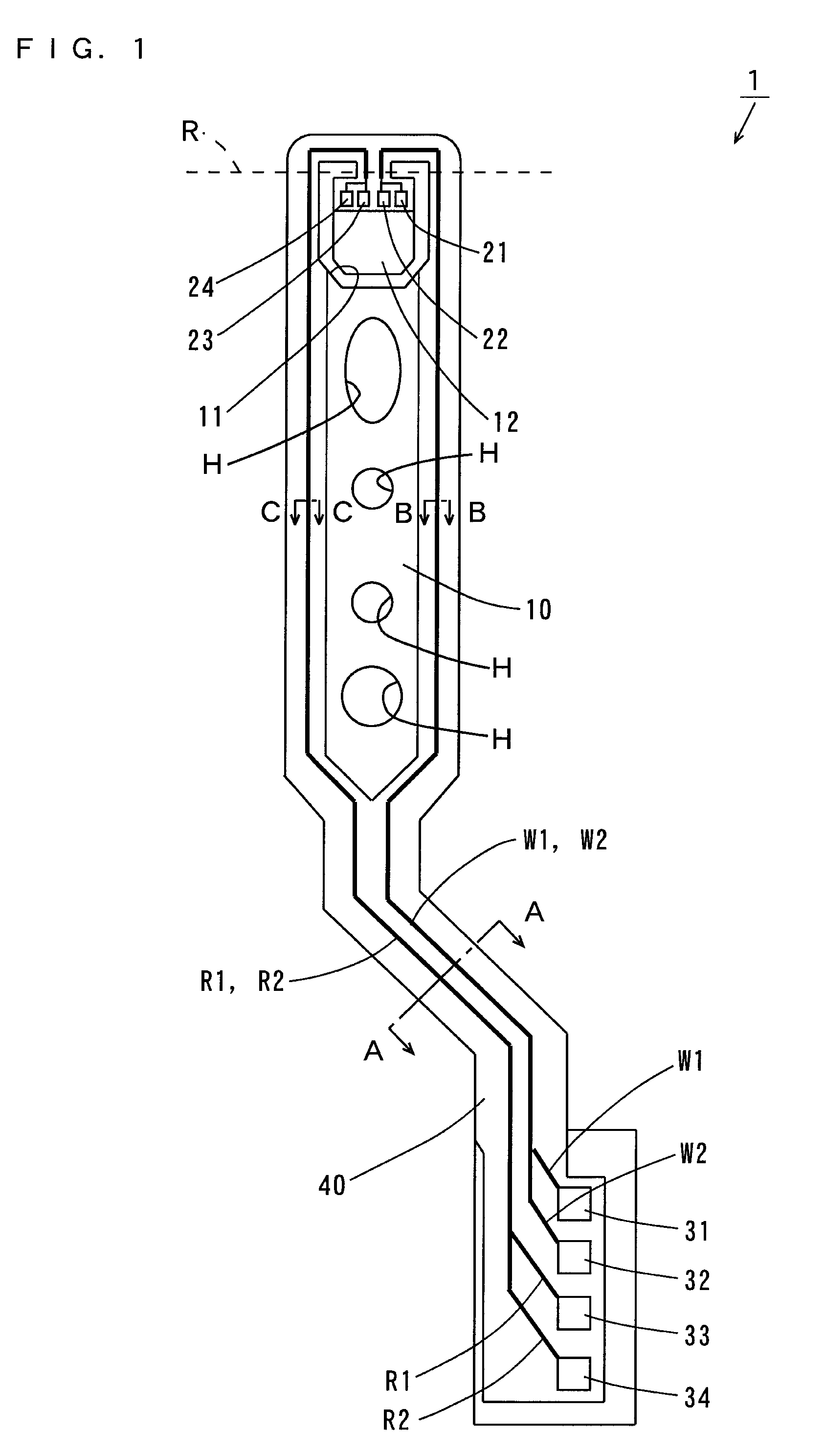
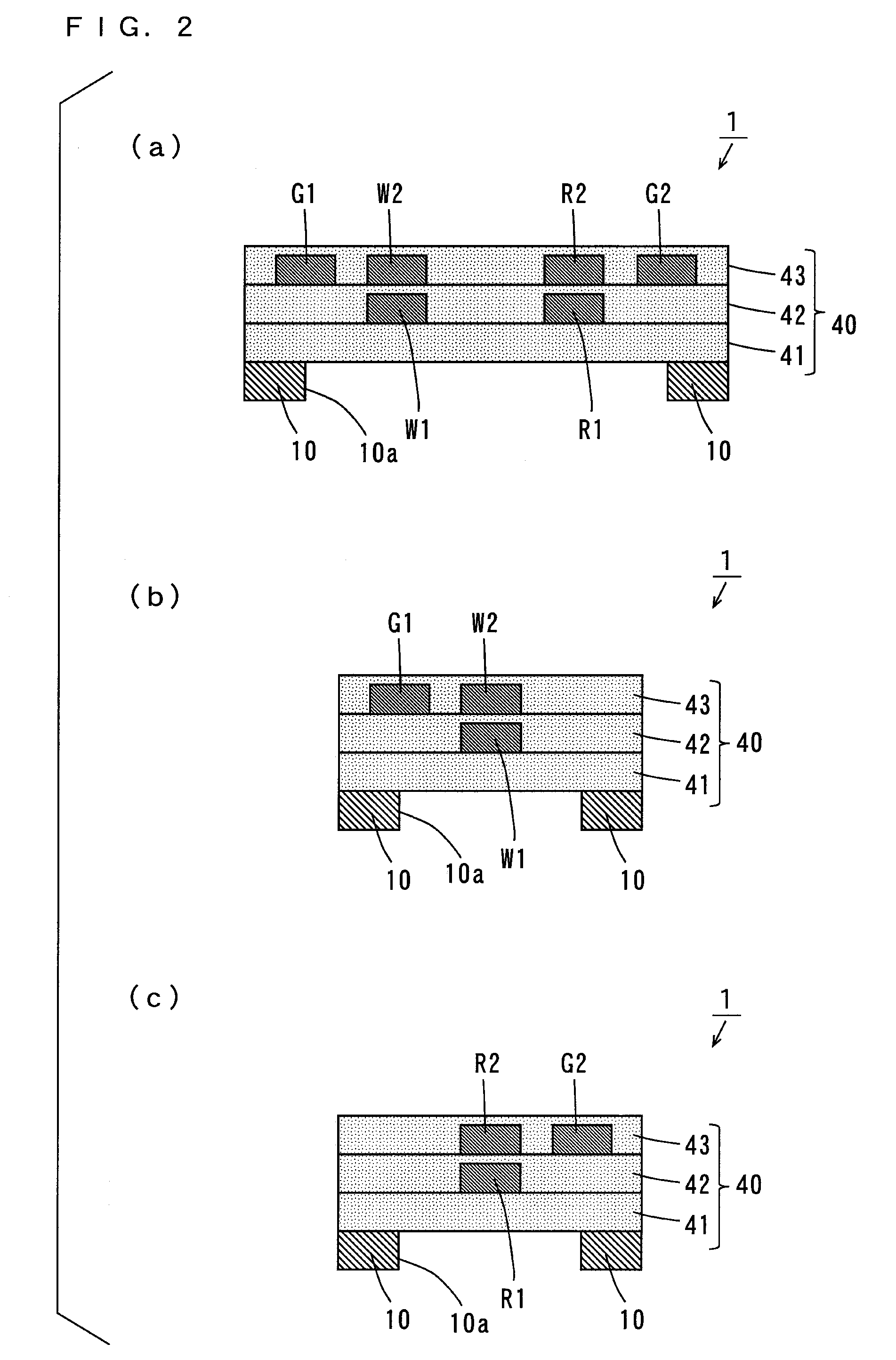
[0053]FIG. 1 is a top view of the suspension board according to a first embodiment of the present invention, and FIG. 2 is a vertical sectional view of the suspension board 1 of FIG. 1. Note that in FIG. 2, (a) shows a sectional view taken along the arrowed line A-A of FIG. 1, (b) shows a sectional view taken along the arrowed line B-B, and (c) shows a sectional view taken along the arrowed line C-C.
[0054]As shown in FIG. 1, the suspension board 1 includes a suspension body 10 formed of a long-sized metal substrate. Write wiring traces W1, W2 and read wiring traces R1, R2 are formed on the suspension body 10 as indicated by the thick solid lines.
[0055]At an end of the suspension body 10, a U-shaped opening 11 is formed, thereby providing a magnetic head supporting portion (hereinafter referred to as a tongue) 12. The tongue 12 is bent along the broken line R to form a predetermined angle with respect to the suspension body 10. Four el...
second embodiment
[0108]FIG. 5 is a vertical sectional view showing a suspension board according to a second embodiment of the present invention. Note that in FIG. 5, (a) shows a sectional view taken along the arrowed line A-A of FIG. 1, (b) shows a sectional view taken along the arrowed line B-B, and (c) shows a sectional view taken along the arrowed line C-C.
[0109]The suspension board 2 according to the present embodiment is different from the suspension board 1 of FIG. 2 in the following points.
[0110]As shown in FIG. 5 (a), in the present embodiment, a ground trace G3 is formed between the write wiring trace W2 and the read wiring trace R2 on the third insulating layer 43 in the sectional view taken along the arrowed line A-A.
[0111]In this case, the ground trace G3 sufficiently prevents occurrence of the crosstalk between the write wiring traces W1, W2 and the read wiring traces R1, R2.
[0112]In addition, the ground trace G3 is formed on the other side of the write wiring trace W2 in the cross sect...
PUM
 Abstract
Description
Claims
Application Information


