Electric-field-effect magnetoresistive devices and electronic devices using the magnetoresistive devices

a technology of electric field effect and magnetoresistive devices, which is applied in the field of electric field effect magnetoresistive devices and electronic devices using magnetoresistive devices, can solve the problems of potential wiring melting problem, unavoidable increase in electrical power consumption, and unavoidable increase in wiring current for writing, so as to achieve good compatibility, control and optimize the mr ratio, the effect of reducing the power consumption required for device operation

Inactive Publication Date: 2007-11-20
HITACHI LTD
View PDF2 Cites 5 Cited by
  • Summary
  • Abstract
  • Description
  • Claims
  • Application Information

AI Technical Summary

Benefits of technology

[0016]In order to resolve the above problems with the related art, a first object of the present invention is to provide an optimized, electrically-controlled magnetoresistance device, further having an improved MR ratio only by using the field effect in FET structures using magnetic materials (for example, diluted magnetic semiconductor) capable of electric-field type of carrier-doping of the substrate, and further provide magnetic sensors of different types or high sensitivity magnetic heads for high density magnetic recording medium utilizing these magnetoresistive devices. A second object of the present invention is to provide an MRAM device having low power consumption and an adequate output signal by utilizing a field effect magnetoresistive device as the means for writing the MRAM memory cells.
[0020]The above described device utilizes the same material in the substrate and therefore has the advantages of no crystal irregularities or defects in the magnetic junction boundary effective in inducing the field effect. In the device structure of the present invention, the MR ratio can be controlled and optimized just by applying a voltage from the gate electrode. Another advantage is that the power consumption required for device operation can be significantly lowered by utilizing the electrical field effect. Further, utilizing a magnetic semiconductor in the substrate will provide good compatibility with conventional semiconductor manufacturing process technology and make integration with peripheral semiconductor circuits simpler.

Problems solved by technology

However, the constantly shrinking size of the memory cell brings about an increase in the magnetic field (magnetic switching field) required for magnetic reversal of the freely magnetized layer that causes an unavoidable increase in the wiring current for writing.
Therefore, increasing the capacity of the MRAM causes an unavoidable increase in electrical power consumption.
The increased electrical current in the wiring brings the potential problem of the wiring melting.
However, this method for inducing a magnetic reversal by injecting a spin current, increases the electrical current density flowing in the TMR device.
This increase in electrical current density might possibly cause the wiring to deteriorate or induce a ferroelectric breakdown in the tunnel insulation (dielectric) due to electro-migration.
However, the internal magnetic semiconductor substrate of this FET is not comprised of a ferromagnetic / nonmagnetic / ferromagnetic junction structure, and so no improvement in the MR ratio can be expected even in the vicinity of the magnetic phase transition.
This FET structure is therefore not suited for use as a magnetoresistive device.
Even though, trial fabrication of ferromagnetic junction type magnetoresistive devices using magnetic semiconductor has also begun very recently, a magnetoresistive device having an MR ratio in excess of 40 percent at room temperature has not been achieved.
However fabricating a satisfactory heterogeneous interface / junction and a uniformly thin intermediate layer is extremely difficult.
Microscopic irregularities at the crystal boundaries of the heterogeneous junction and the effects of microscopic pin holes formed unintentionally in the nonmagnetic intermediate layer create the problem that the MR ratio of the magnetoresistance device drastically deteriorates from the theoretically expected value.
Further, the MR ratio in the magnetoresistive device, varies according to the film thickness of the nonmagnetic intermediate layer so that obtaining a large improvement in the MR ratio and optimizing with the peripheral circuits could only be achieved by experimentally fabricating large numbers of devices with nonmagnetic layers of different film thickness.

Method used


Image

  • Electric-field-effect magnetoresistive devices and electronic devices using the magnetoresistive devices
  • Electric-field-effect magnetoresistive devices and electronic devices using the magnetoresistive devices
  • Electric-field-effect magnetoresistive devices and electronic devices using the magnetoresistive devices

Examples


first embodiment

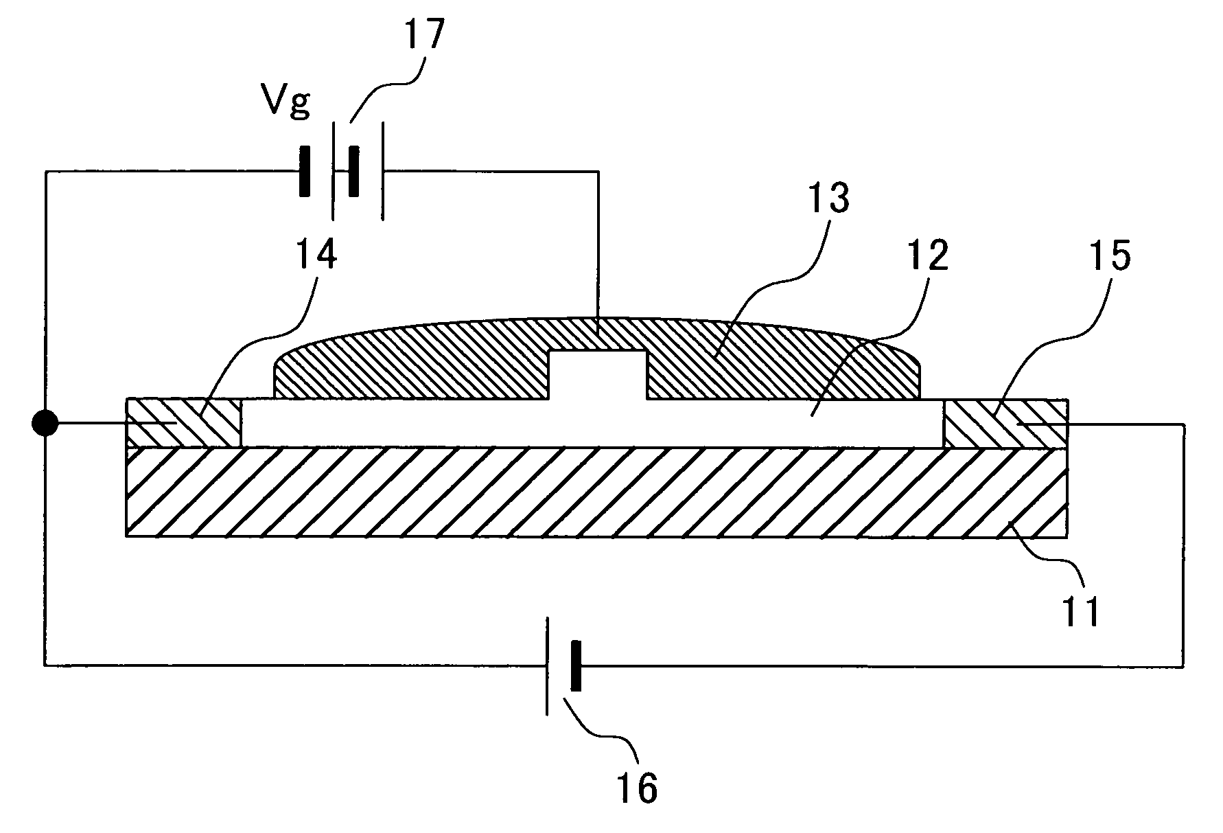
[0035]FIG. 1A is a cross sectional view showing the FET structure of the field effect magnetoresistance device of the first embodiment. An electrical insulating layer 12 whose structure is patterned in a convex shape is formed on the upper part of the nonmagnetic substrate 11 capable of being doped with electric field carriers. A first metallic electrode (gate electrode) 13 is formed on the insulating (film) layer 12. When an external section applies a positive voltage of Vg>0 to the gate electrode 13 from the power supply 17, a strong electrical field is applied locally to the substrate directly below the region where the insulating film layer is thin and that part of the substrate can be doped with a high concentration of hole carriers (doped region with high concentration of carriers is formed). On the other hand, when a weak electrical field is applied to the region on the substrate directly below region where the insulating film is thick, then that part of the substrate can be ...

second embodiment

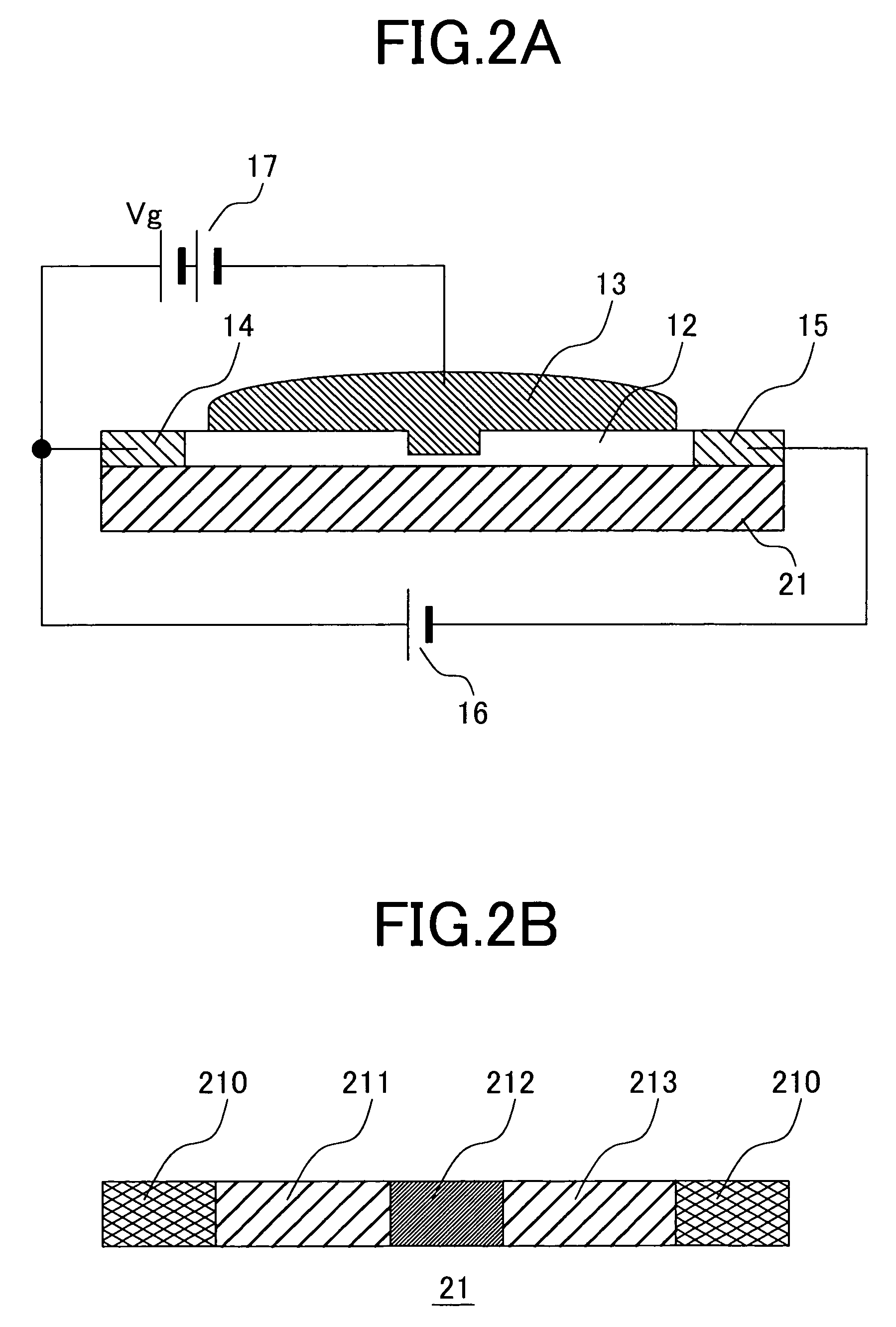
[0042]The FET structure of the field effect magnetoresistance device of the first embodiment can also be achieved with a ferromagnetic substrate capable of being electric carrier doped rather than by a non-magnetic substrate capable of being doped with electrical field carriers. In other words, a ferromagnetic domain / nonmagnetic domain / ferromagnetic domain junction structure possessing functions identical to the first embodiment can be achieved even by a ferromagnetic substrate capable of being doped with electric field carriers.

[0043]FIG. 2A is a cross sectional view showing the FET structure of the field effect magnetoresistance device of the second embodiment. Sections identical to the first embodiment of FIG. 1A are assigned the same reference numerals. Comparing FIG. 2A with FIG. 1A clearly shows that an electric field carrier dopable ferromagnetic substrate 21 is utilized instead of the electric field carrier dopable nonmagnetic substrate 11. This comparison also shows that a ...

third embodiment

[0046]A multijunction GMR device or TMR device and its multiple circuits can easily be formed on the substrate by combining the detailed patterning of the insulating layer 12 of the first embodiment or the second embodiment and the MR ratio can be further improved. FIG. 4A is a cross sectional view showing the multi-joint structure of the FET structure of the first embodiment. FIG. 4B is a cross sectional view of the ferromagnetic domain / nonmagnetic domain / ferromagnetic domain multi-junction structure. In FIG. 4B, the reference numerals 111 and 113 should be assigned to the ferromagnetic domains between two nonmagnetic domains 112; however, to avoid complexity, one number was assigned.

[0047]When comparing the magnetoresistance of the magnetoresistance device comprising the above described multijunction GMR device or TMR device with the simple device shown in FIG. 3, the multijunction quantity is set as n, and the total series-connected magnetoresistance is found to be improved n tim...


PUM

PropertyMeasurementUnit
thicknessaaaaaaaaaa
thicknessaaaaaaaaaa
thicknessaaaaaaaaaa

Abstract

Magnetoresistive devices with increased response sensitivity to external magnetic fields and an increased magnetoresistive ratio (MR ratio) to cope with rapid advances made in a highdensity magnetic recording device. A patterned dielectric layer is laminated in a flat shape on a substrate capable of being doped with carriers (holes) in an electric field, and an FET structure with gate electrodes is then fabricated on that dielectric layer, and the substrate spatially modulated by applying a nonuniform electrical field to induce a first ferromagnetic domain, a nonmiagnetic domain and a second ferromagnetic domain.

Description

CLAIM OF PRIORITY[0001]The present application claims priority from a Japanese application JP 2003-176293 filed on Jun. 20, 2003, the content of which is hereby incorporated by reference into this application.FIELD OF THE INVENTION[0002]The present invention relates to laminated magnetoresistance devices containing a ferromagnetic layer, nonmagnetic layer, ferromagnetic layer and to electronic devices using these magnetoresistance devices.BACKGROUND OF THE INVENTION[0003]The magnetoresistance effect is generally a physical phenomenon wherein a magnetic field is applied to a magnetic material to vary the electrical resistance. The GMR device that utilizes the giant magnetoresistance (GMR) effect discovered in metallic multilayer film structures comprised of laminations of ferromagnetic metal layers / nonmagnetic metal layers / ferromagnetic metal layers is already utilized in magnetic read-out heads. In recent years, the application of magnetic random access memory (MRAM) devices as nonv...

Claims


Application Information

Patent Timeline
Patent Type & Authority Patents(United States)
IPC IPC(8): G11B5/127G01R33/09G11B5/33G11B5/37G11B5/39G11C11/14G11C11/15G11C19/08H01L21/8246H01L27/105H01L43/08
CPCB82Y10/00B82Y25/00G01R33/093G11B5/332G11B5/376H01L43/08G11B5/3993G11C11/14G11C19/0808G11B5/3903G11B2005/3996H10N50/10
Inventor ONOGI, TOSHIYUKIICHIMURA, MASAHIKOHASHIZUME, TOMIHIRO
Owner HITACHI LTD
Why Eureka
Try Eureka