Electronic component mounting system and electronic component mounting method

a technology for electronic components and mounting systems, applied in the direction of printed circuit manufacture, metal working apparatus, manufacturing tools, etc., can solve the problems of difficult to effectively prevent mounting defects, and the inability to appropriately deposited electronic components at mounting points on the substra

Inactive Publication Date: 2011-09-20
PANASONIC CORP
View PDF20 Cites 7 Cited by
  • Summary
  • Abstract
  • Description
  • Claims
  • Application Information

AI Technical Summary

Benefits of technology

[0007]One objective of the present invention is, therefore, to provide an electronic component mounting system and an electronic component mounting method that can prevent a mounting defect due to a positioning error in the direction of the thickness of a substrate, and that can deliver a specific mounting quality.
[0010]According to the present invention, a substrate height measurement apparatus measures the heights at height measurement points, designated on the upper face of a substrate, and outputs the measurement results as substrate height data. Then, once the substrate has been delivered to an electronic component placing apparatus, the substrate height measurement apparatus again measures the height of the substrate at specific height measurement points to obtain substrate height correction data, and based on the initial substrate height data and the substrate height correction data, update a control parameter for controlling the component placing operation performed by a loading head. In this manner, discrepancies in the positions of the heights of individual substrates can be accurately corrected, and mounting defects due to positioning errors in the direction of the heights of the substrates can be prevented.

Problems solved by technology

Therefore, when a variance in the thickness of a substrate is encountered, or when the substrate has been deformed by warping, an electronic component can not be appropriately deposited at a mounting point on the substrate, and this becomes a factor in the occurrence of a mounting defect such as a position shift.
As described above, with the conventional mounting system, it is difficult to effectively prevent a mounting defect that is the result of a positioning error in the direction of the thickness of a substrate.

Method used


Image

  • Electronic component mounting system and electronic component mounting method
  • Electronic component mounting system and electronic component mounting method
  • Electronic component mounting system and electronic component mounting method

Examples


Embodiment Construction

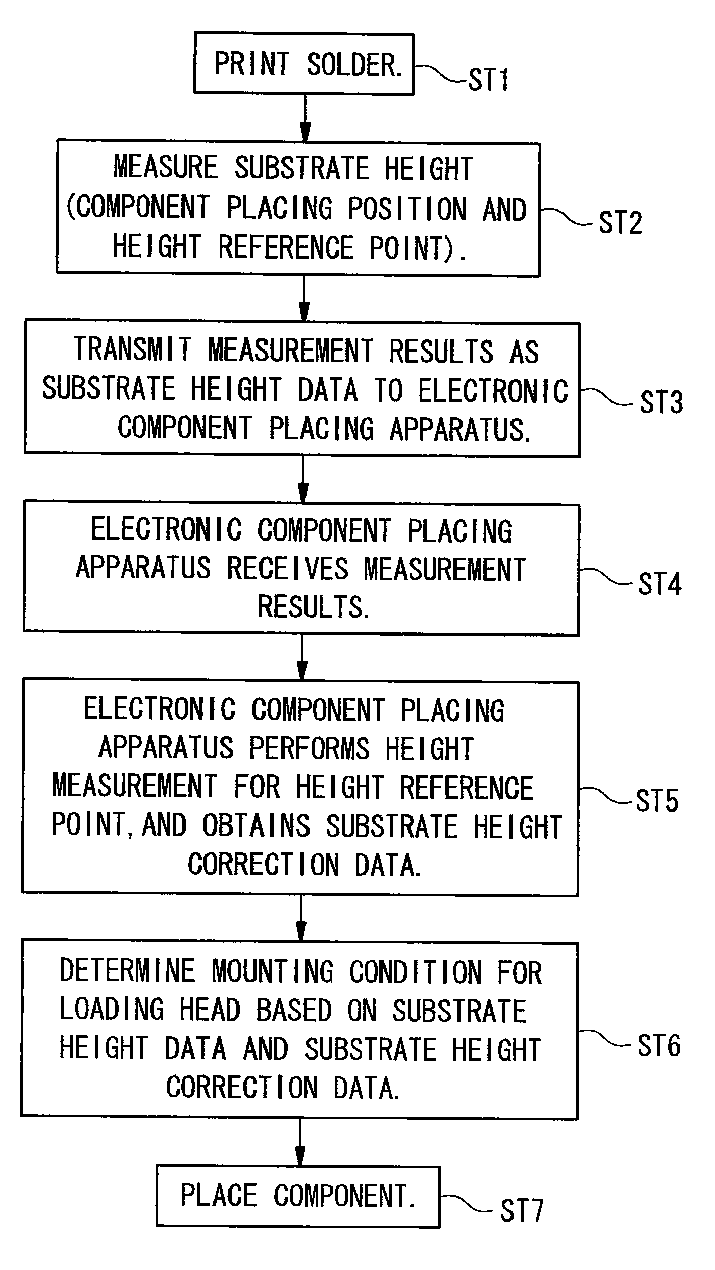
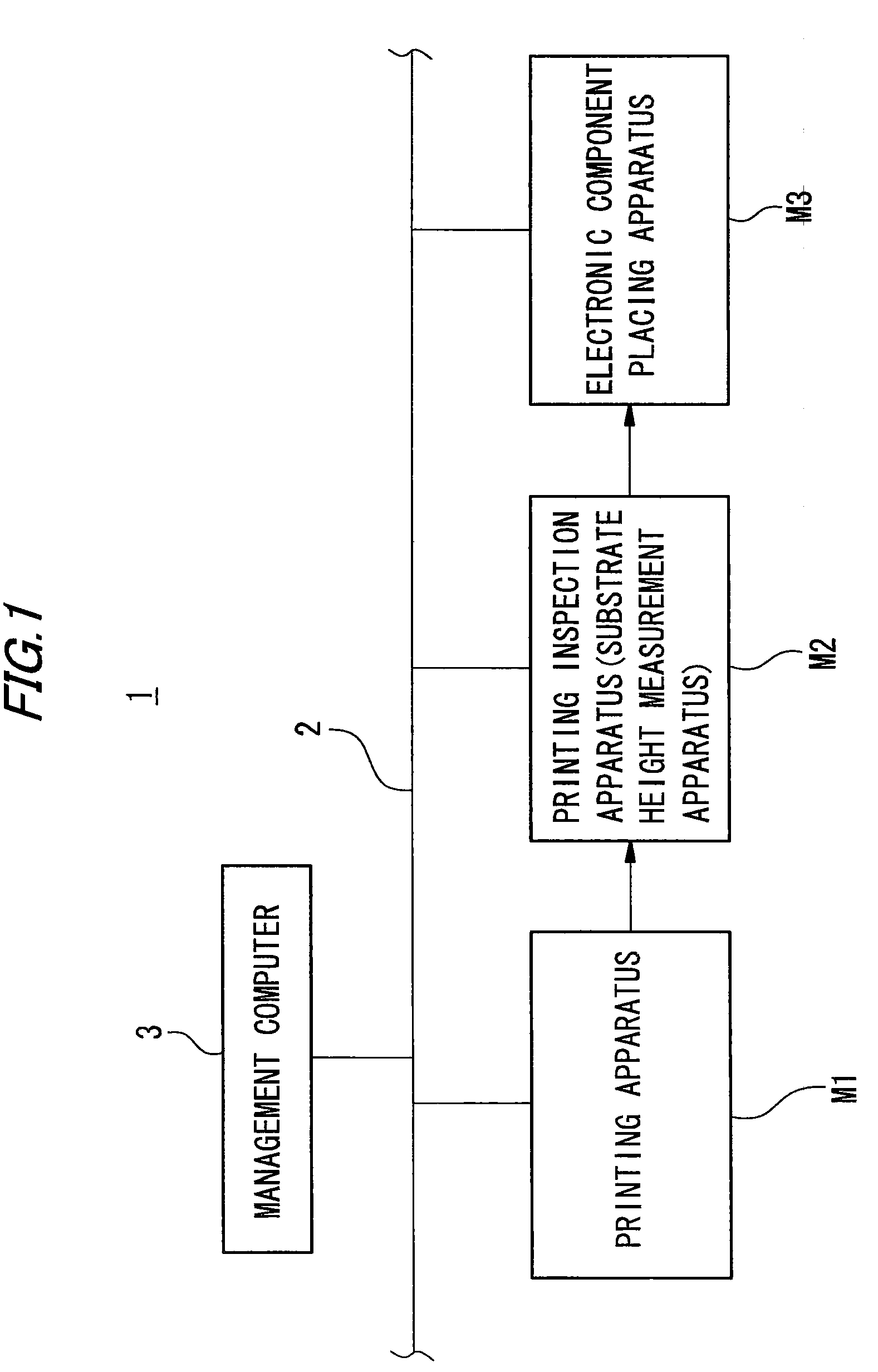
[0022]One embodiment of the present invention will now be described. First, the electronic component mounting system will be described while referring to FIG. 1. In FIG. 1, for the electronic mounting system, an electronic component mounting line 1 is formed by connecting together a printing apparatus M1, a printing inspection apparatus M2 and an electronic component placing apparatus M3, all of which apparatuses are used for mounting electronic components, and is connected to a management computer 3, via a communication network 2, so that the computer 3 can control the entire system. By using these electronic component mounting apparatuses, electronic components can be mounted on a substrate, and a components mounting substrate can be produced.

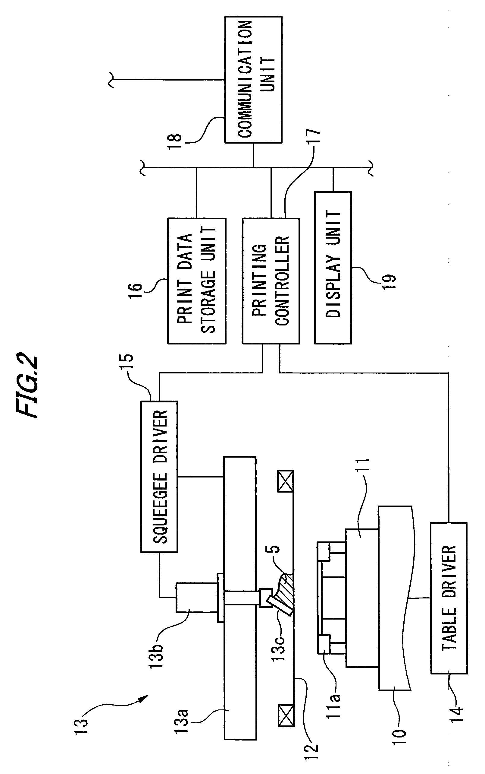
[0023]The printing apparatus M1 performs screen printing for the electrodes of a substrate using a solder paste employed to bond electronic components. The printing inspection apparatus M2 inspects the printing condition of the printed solder...


PUM

PropertyMeasurementUnit
heightsaaaaaaaaaa
heightaaaaaaaaaa
substrate height measurementaaaaaaaaaa

Abstract

One objective of the present invention is to provide an electronic component mounting system and an electronic component mounting method that can prevent a mounting defect due to a positioning error in the direction of the thickness of a substrate, and that can deliver a specific mounting quality. According to an electronic component mounting system, which is constituted by coupling a plurality of apparatuses used for mounting electronic components, the height measurement device 22 of a printing inspection apparatus measures the heights at height measurement points, designated on the upper face of a substrate, and outputs the measurement results as substrate height data. Then, once the substrate has been delivered to an electronic component placing apparatus, the substrate height measurement apparatus again measures the height of the substrate at specific height measurement points to obtain substrate height correction data, and based on the initial substrate height data and the substrate height correction data, updates a control parameter for controlling the component placing operation performed by a loading head. In this manner, discrepancies in the positions of the heights of individual substrates can be accurately corrected, and mounting defects due to positioning errors in the direction of the heights of the substrates can be prevented.

Description

TECHNICAL FIELD[0001]The present invention relates to an electronic component mounting system and an electronic component mounting method for mounting electronic components on a substrate.BACKGROUND ART[0002]An electronic component mounting system, which uses soldering to mount electronic components on a substrate and to produce a components mounting substrate, is constituted by connecting together a plurality of apparatuses used for mounting electronic components, such as a solder printing apparatus, an electronic component placing apparatus and a reflow soldering apparatus. In order to perform reliable quality control for the electronic component mounting system, an electronic component mounting line equipped with an inspection function is introduced, so that an inspection apparatus is arranged between individual apparatuses (see, for example, patent document 1).[0003]In the example in this patent document 1, a printing inspection apparatus is arranged between the printing apparat...

Claims


Application Information

Patent Timeline
Patent Type & Authority Patents(United States)
IPC IPC(8): H05K3/36H05K3/20
CPCH05K13/08Y10T29/49128Y10T29/4913Y10T29/53174H05K13/082H05K13/04
Inventor INOUE, MASAFUMITSUKAMOTO, MITSUHAYANISHI, SYOICHIKIHARA, MASAHIRO
Owner PANASONIC CORP
Why Eureka
Try Eureka