Trench metal oxide semiconductor field effect transistor (MOSFET) with low gate to drain coupled charges (Qgd) structures

a technology of metal oxide semiconductor and field effect transistor, which is applied in the field of low gate and low gate configuration manufacturing methods for fabricating semiconductor power devices, can solve the problems of large amount of coupling charges qgd, complicated device structure formation, and high cost, and achieve the effect of reducing the coupling charge between the gate and the drain

Active Publication Date: 2011-09-20
FORCE MOS TECH CO LTD
View PDF3 Cites 12 Cited by
  • Summary
  • Abstract
  • Description
  • Claims
  • Application Information

AI Technical Summary

Benefits of technology

[0007]It is therefore an aspect of the present invention to provide a new and improved semiconductor power device by forming P* dopant regions surrounding the lower portions of the gate sidewalls to decouple the gate from the drain such that the coupling charges between the gate and the drain can be reduced. Furthermore, a N* dopant region is formed right below the trench bottom to provide a current path between the drain to the source such that the decoupling P* dopant regions will not inadvertently increase the drain to source resistance but Crss can be significantly reduced to a capacitance that is about half or even lower when compared with the capacitance of the conventional devices because the Crss will be mainly determined by trench width in the present invention when compared with the conventional device as shown in FIG. 1.
[0008]Another aspect of this invention is to form an improved MOSFET device by forming P* dopant regions surrounding the lower portions of the gate sidewalls to reduce the gate-to-drain coupling charges and N* regions below the bottom of the trenches to provide a drain to current path. Furthermore, the improved MOSFET device is formed with thicker oxide layer at the bottom of the trenched gate such that the gate to drain capacitance can be reduced. The performance of the device is improved with reduced Qgd by reducing the coupling areas between the gates to the drain. The drain to source resistance is reduced with a current path provided by the N* dopant regions below the bottom of the trenches.

Problems solved by technology

However, conventional device as shown in FIG. 1 has a large amount of coupling charges Qgd between the gates and drain due to the direct coupling between the sidewalls of the trench gates and the drain.
However, formation of the device structures is very complicate and expensive.

Method used


Image

  • Trench metal oxide semiconductor field effect transistor (MOSFET) with low gate to drain coupled charges (Qgd) structures
  • Trench metal oxide semiconductor field effect transistor (MOSFET) with low gate to drain coupled charges (Qgd) structures
  • Trench metal oxide semiconductor field effect transistor (MOSFET) with low gate to drain coupled charges (Qgd) structures

Examples


Embodiment Construction

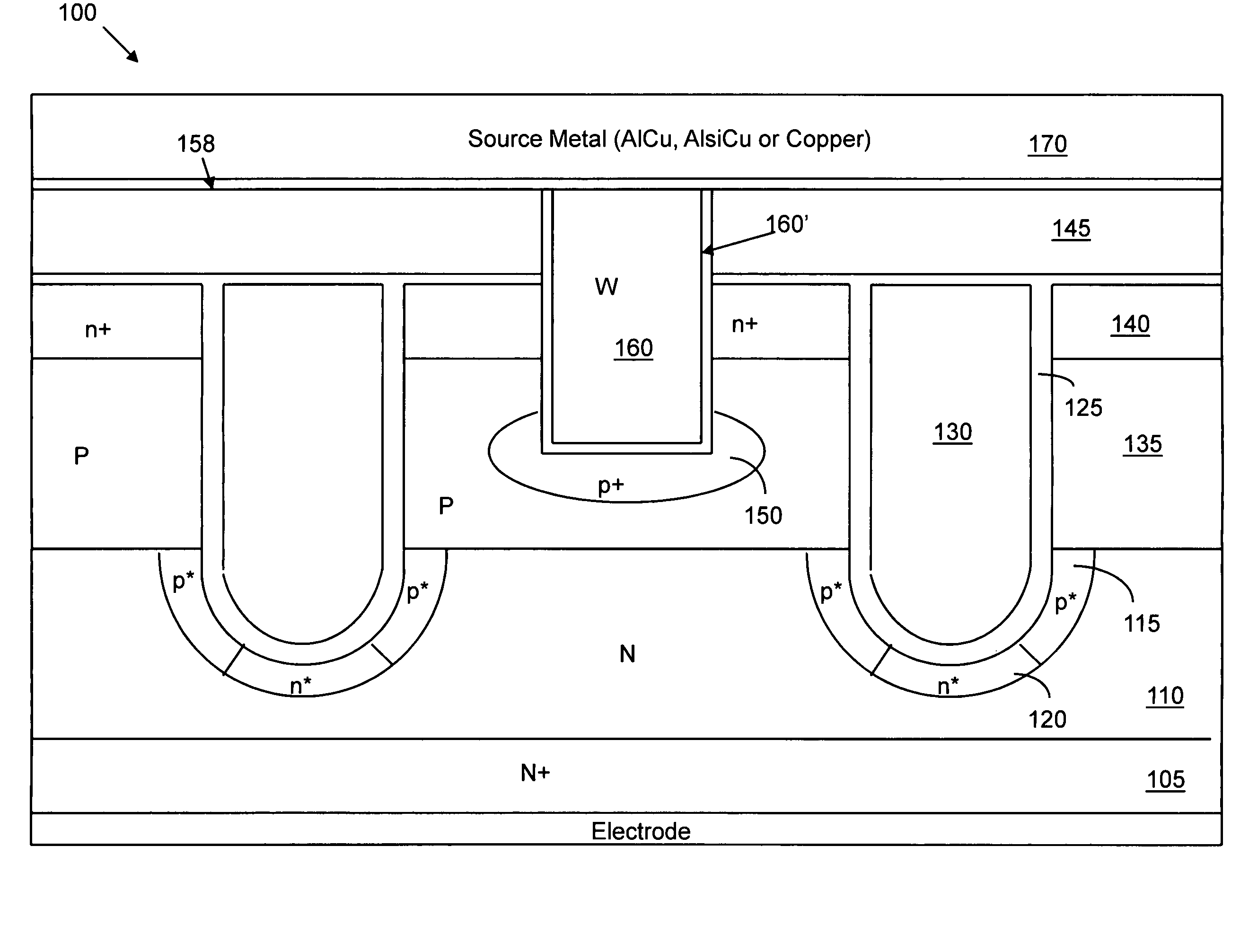
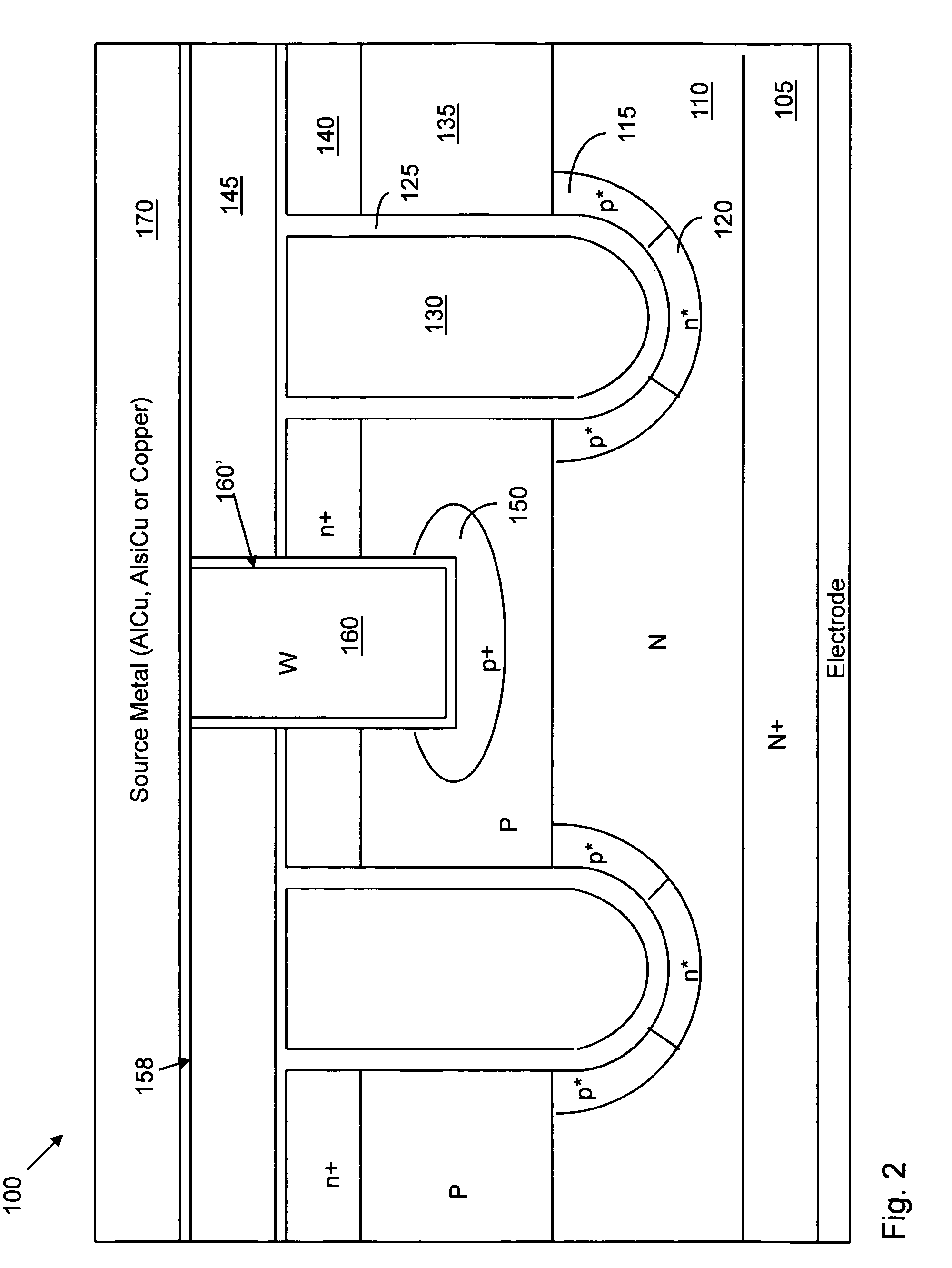
[0015]Referring to FIG. 2 for a side cross sectional view of a MOSFET device 100 formed on a N+ substrate 105 supporting an N-epitaxial layer 110 with trenched polysilicon gates 130. Each of these trenched gates 130 is padded by a gate oxide layer 125. A plurality of P-body regions 135 disposed on the upper portion of the epitaxial layer 110 surround the trenched gates 130. The body regions 135 further encompassed source regions 140 formed near the top surface of the epitaxial layer 110 surrounding the trenched gates 130. An oxide insulation layer 145 covering the top surface with contact openings right above the contact enhancing dopant regions 150 are opened through the insulation layer to allow for the metal contact layer 170 to physically contact the source / body regions through a resistance reduction layer 158 to the contact enhancing regions 150. The contact trenches 160 are filled with tungsten contact plugs padded with a barrier layer 160′ composed of Ti / TiN. The resistance r...


PUM


Abstract

A trenched semiconductor power device includes a plurality of trenched gates surrounded by source regions near a top surface of a semiconductor substrate encompassed in body regions. The trenched semiconductor power device further comprises tilt-angle implanted body dopant regions surrounding a lower portion of trench sidewalls for reducing a gate-to-drain coupling charges Qgd between the trenched gates and a drain disposed at a bottom of the semiconductor substrate. The trenched semiconductor power device further includes a source dopant region disposed below a bottom surface of the trenched gates for functioning as a current path between the drain to the source for preventing a resistance increase caused by the body dopant regions surrounding the lower portions of the trench sidewalls.

Description

BACKGROUND OF THE INVENTION[0001]1. Field of the Invention[0002]The invention relates generally to the device configuration and manufacturing methods for fabricating the semiconductor power devices. More particularly, this invention relates to an improved and novel manufacturing process and device configuration for reducing the gate to drain coupled charges (Qgd) while providing a drain to source current path for preventing a drain to source resistance.[0003]2. Description of the Related Art[0004]In order to increase the switching speed of a semiconductor power device, it is desirable to reduce the coupling charges between the gates and drain Qgd such that a reduction of a gate to drain capacitance Crss can be reduced. However, conventional device as shown in FIG. 1 has a large amount of coupling charges Qgd between the gates and drain due to the direct coupling between the sidewalls of the trench gates and the drain. Specifically, Kobayashi discloses in a U.S. Pat. No. 6,888,196 en...

Claims


Application Information

Patent Timeline
Patent Type & Authority Patents(United States)
IPC IPC(8): H01L29/76
CPCH01L29/1095H01L29/66727H01L29/66734H01L29/7813H01L29/0878H01L29/41766H01L29/42368H01L29/456H01L21/26586
Inventor HSHIEH, FWU-IUAN
Owner FORCE MOS TECH CO LTD
Why Eureka
Try Eureka