
Multilayer wiring board and method of manufacturing the same

a wiring board and multi-layer technology, applied in the direction of printed circuit manufacturing, printed circuit aspects, programmable/customizable/modifiable circuits, etc., can solve the problems of small wiring pitch on the board, large occupied connection pads, and bottlenecks, and achieve high-density wiring

Active Publication Date: 2011-09-27
SHINKO ELECTRIC IND CO LTD
View PDF8 Cites 2 Cited by
  • Summary
  • Abstract
  • Description
  • Claims
  • Application Information

AI Technical Summary

Benefits of technology

This configuration allows for high-density wiring by enabling closer routing of wiring patterns and ensures reliable electrical connections between boards, even with minor misalignment during stacking, by forming an integral structure with overlapping fin-shaped bumps.

Problems solved by technology

However, such a connection pad forms a bottleneck in high-density wiring under recent circumstances where a wiring pitch on board has become small.
Specifically, an area occupied by the connection pads is becoming relatively large, resulting in a problem in that the connection pad 9 causes an obstruction to wiring, for example, as shown in FIG. 8, due to being bottlenecked on its size.
The connection pad is disadvantageous in the high-density wiring, because higher wiring density, in particular, leads to a higher percentage of occupation by the connection pads (specifically, a larger area occupied by the connection pads and also a larger number of connection pads installed).
Also encountered is a problem in that the connection pad does not necessarily provide an electrical interconnection between the boards (or the wiring patterns) therethrough, depending on the degree of misalignment or the like.

Method used


Image

  • Multilayer wiring board and method of manufacturing the same
  • Multilayer wiring board and method of manufacturing the same
  • Multilayer wiring board and method of manufacturing the same

Examples


Embodiment Construction

[0026]Description will be given below with regard to preferred embodiments of the present invention with reference to the accompanying drawings.

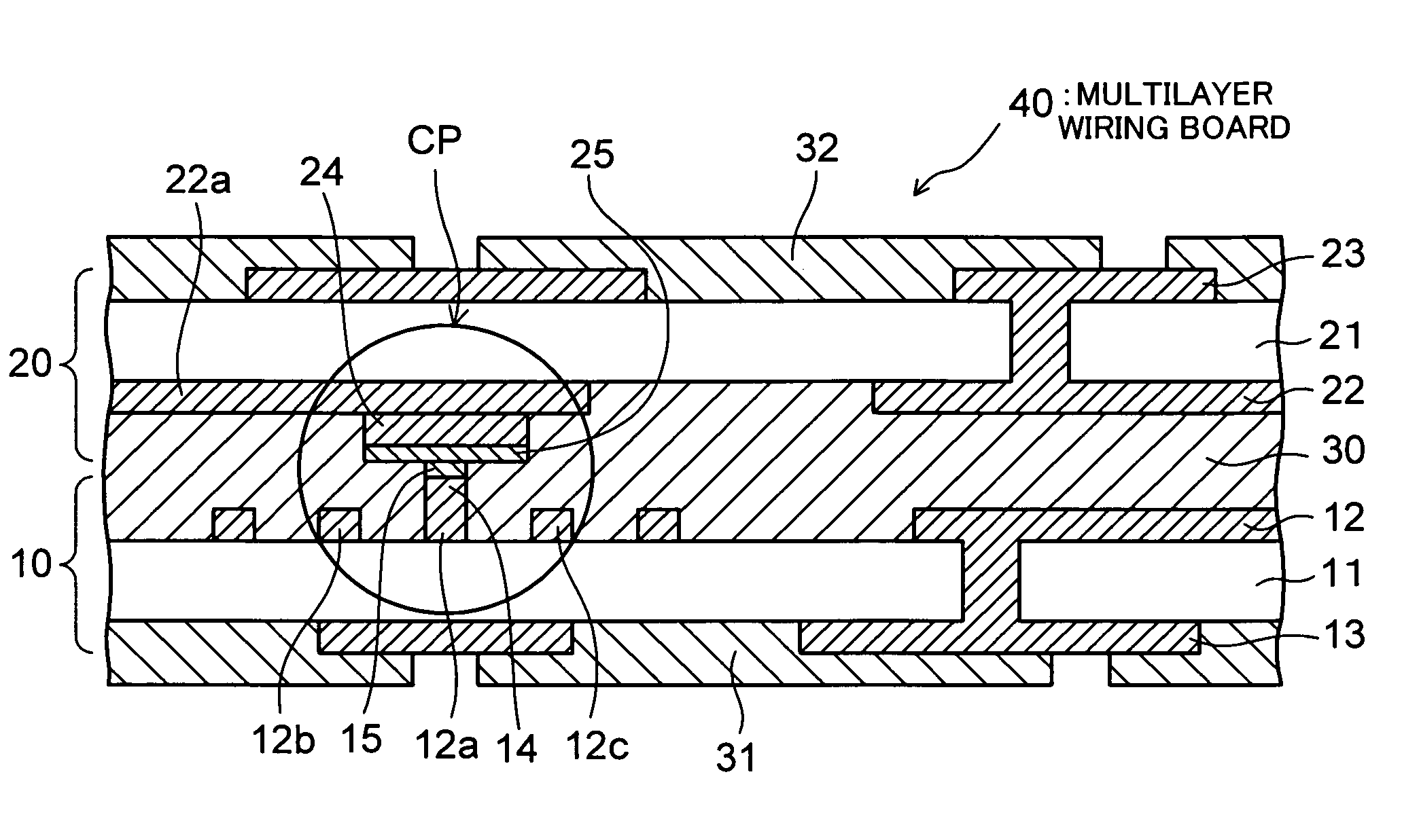
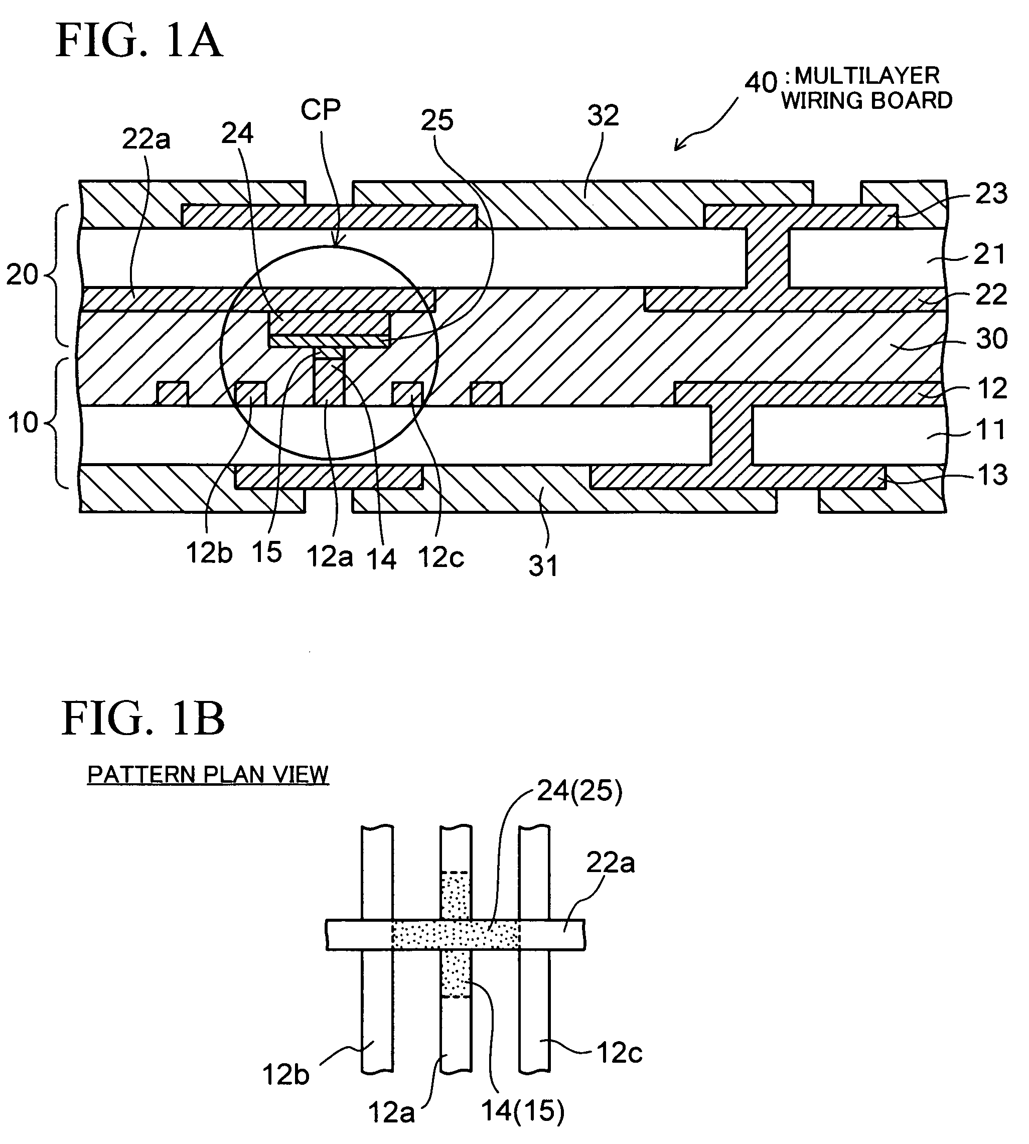
[0027]FIGS. 1A and 1B show the configuration of a multilayer wiring board according to an embodiment of the present invention. FIG. 1A shows its structure in cross section, and FIG. 1B shows, in plan view, the configuration (or pattern) of its principal part (specifically a circled part indicated by reference character CP in FIG. 1A, namely, a “cross post section” to be described later).

[0028]As shown in FIG. 1A, the multilayer wiring board 40 according to the embodiment includes two wiring boards 10 and 20 stacked up vertically, an insulating layer 30 formed to be filled between the wiring boards 10 and 20, and insulating layers 31 and 32 functioning as protection films formed on the outermost layers of the board 40. The wiring boards 10 and 20 have resin substrates 11 and 21 as base members, and on both sides thereof, wiring layers 12 and ...


PUM

PropertyMeasurementUnit
thickaaaaaaaaaa
thickaaaaaaaaaa
thicknessaaaaaaaaaa

Abstract

A multilayer wiring board includes at least two wiring boards having wiring layers containing wiring patterns formed on both sides. A pair of fin-shaped bumps are formed at desired positions on wiring patterns on the surfaces facing each other, of the wiring boards, so that the bumps assume a slender shape as seen in plan view and that the bumps intersect each other. The pair of fin-shaped bumps are electrically connected to form an inter-board connection terminal. Further, an insulating layer is formed between the wiring boards, and protection films are formed to cover the entire surface except pad areas defined at predetermined positions on outer wiring layers of the wiring boards.

Description

CROSS-REFERENCE TO RELATED APPLICATIONS[0001]This application is based on and claims priority of Japanese Patent Application No. 2007-026540 filed on Feb. 6, 2007, the entire contents of which are incorporated herein by reference.BACKGROUND OF THE INVENTION[0002](a) Field of the Invention[0003]The present invention relates to a technique of manufacturing a wiring board for use in mounting of a chip component such as a semiconductor device, and more particularly to a multilayer wiring board having a multilayer structure adapted to achieve high density and a method of manufacturing the same.[0004](b) Description of the Related Art[0005]To fabricate a wiring board of multilayer structure formed of a plurality of wiring boards stacked up with an insulating adhesive layer such as prepreg being provided therebetween, various approaches and technologies have been heretofore used as methods of interconnecting wiring patterns formed on the wiring boards. For example, FIG. 7A shows one of the...

Claims


Application Information

Patent Timeline
Patent Type & Authority Patents(United States)
IPC IPC(8): H05K1/03
CPCH05K3/462H05K3/4647H05K1/0289Y10T29/49126H05K2203/0733H05K2203/1327H05K2201/09245H05K3/46
Inventor TANAKA, KOICHI
Owner SHINKO ELECTRIC IND CO LTD
Learn More