
Semiconductor chip module with stacked flip-chip unit

a technology of semiconductor chip module and flip-chip unit, which is applied in the field of chip modules, can solve the problems of reducing the integration of the semiconductor chip module package b>1/b>, reducing and prolonging the manufacturing time. , to achieve the effect of reducing the thickness, reducing the size of the stacked chips, and enhancing the adaptability of the manufacturing process

Active Publication Date: 2011-09-27
PANELSEMI CORP
View PDF10 Cites 0 Cited by
  • Summary
  • Abstract
  • Description
  • Claims
  • Application Information

AI Technical Summary

Benefits of technology

This approach reduces the size of the chip module, enhances manufacturing adaptability, and increases product reliability by eliminating the need for wire bonding and allowing for thinner flip-chip units, thereby improving integration and yield.

Problems solved by technology

However, the size of the bonding head is large and the disposition of the wires W needs a certain height and distance, such that the spacer 13 is needed to increase the height and the distance between the chips 12 and 14 so to facilitate the movement of the bonding head and the disposition of the wires W. Nonetheless, it also reduces the integration of the semiconductor chip module package 1.
This reduces the adaptability of the manufacturing process and extends the manufacturing time.
Additionally, the yield and the reliability of the product may be reduced since the wires in the wire-bonded products may be easily broken, which results in the malfunctions of the products.

Method used


Image

  • Semiconductor chip module with stacked flip-chip unit
  • Semiconductor chip module with stacked flip-chip unit
  • Semiconductor chip module with stacked flip-chip unit

Examples


Embodiment Construction

[0026]The present invention will be apparent from the following detailed description, which proceeds with reference to the accompanying drawings, wherein the same references relate to the same elements.

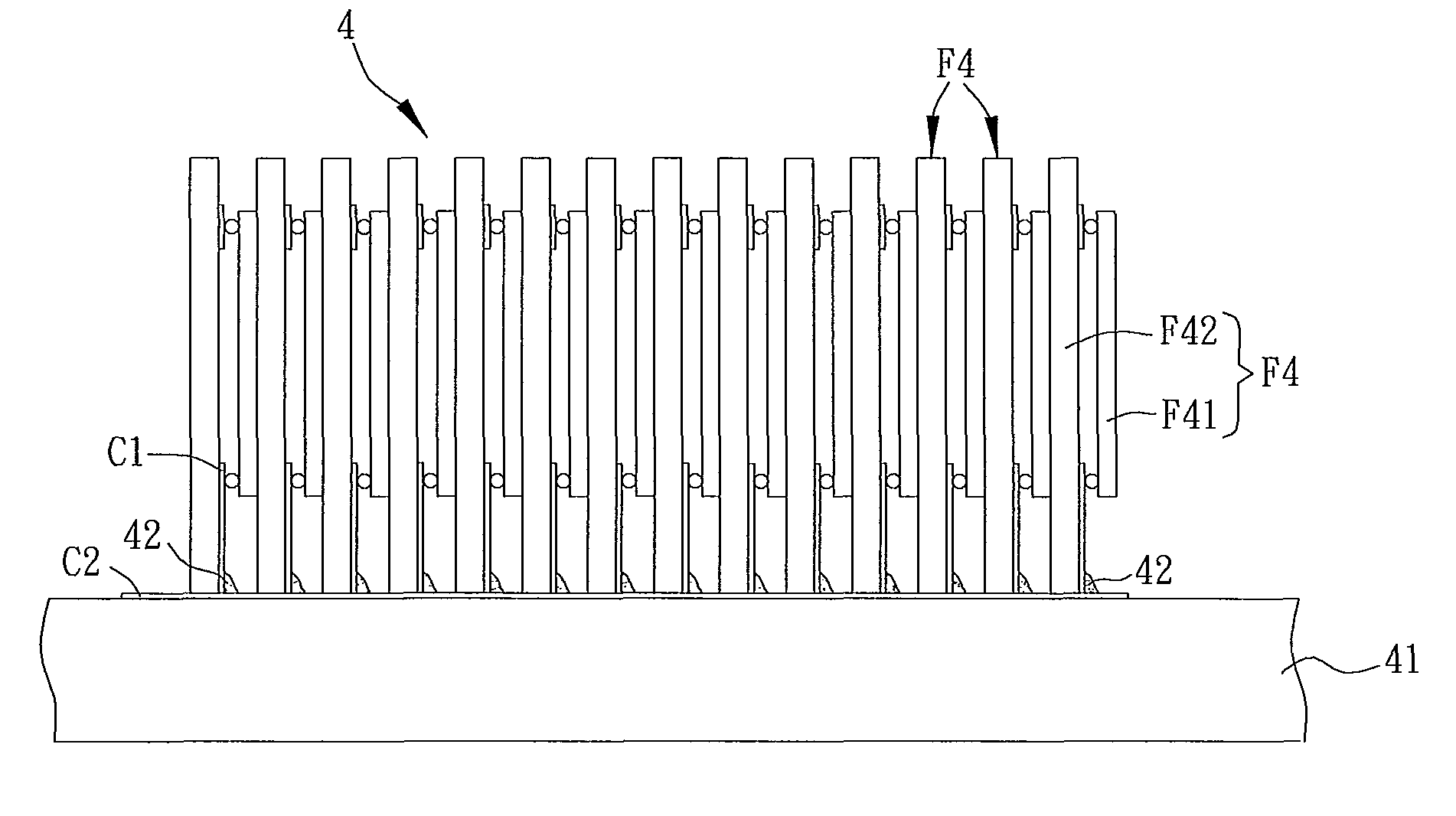
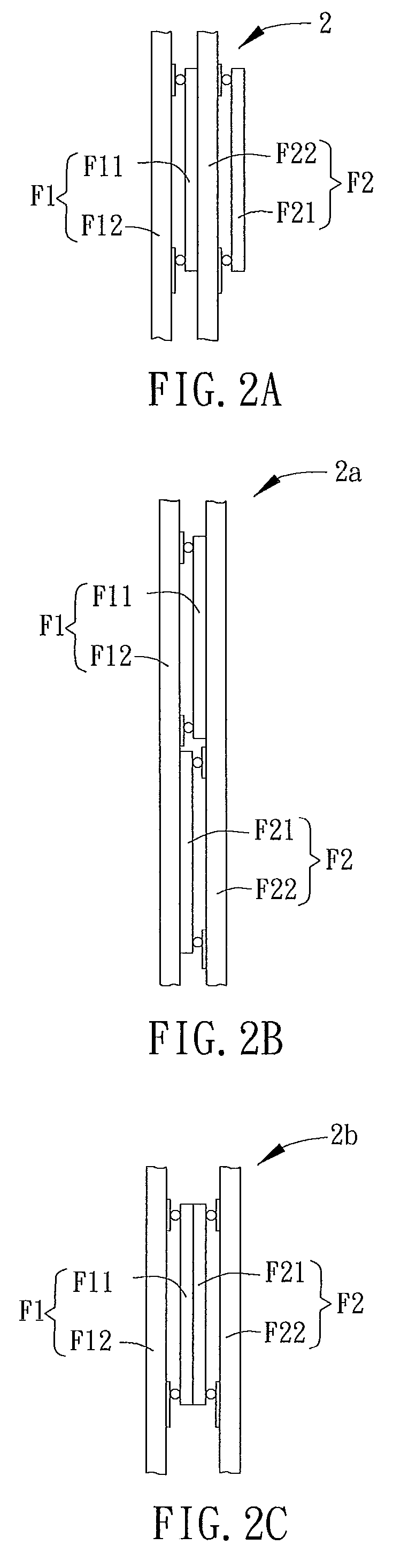
[0027]FIG. 2A is a schematic view of a semiconductor chip module 2 according to a preferred embodiment of the present invention. The semiconductor chip module 2 includes a first flip-chip unit F1 and a second flip-chip unit F2.

[0028]The first flip-chip unit F1 includes a first chip F11 and a first glass circuit board F12. The first chip is connected to the first glass circuit board F12 by flip-chip bonding. The second flip-chip unit F2 has a second chip F21 and a second glass circuit board F22. The second chip F21 is connected to the second glass circuit board F22 by flip-chip bonding. The first flip-chip unit F1 and the second flip-chip unit F2 are attached to each other by, for example, an adhesive.

[0029]In the embodiment, the first chip F11 and / or the second chip F21 may be a die, ...


PUM


Abstract

A semiconductor chip module includes a first flip-chip unit and a second flip-chip unit. The first flip-chip unit has a first chip and a first glass circuit board. The first chip is connected with the first glass circuit board by flip-chip bonding. The second flip-chip unit has a second chip and a second glass circuit board. The second chip is connected with the second glass circuit board by flip-chip bonding. The first flip-chip unit and the second flip-chip unit are attached to each other. A method for manufacturing the semiconductor chip module is also disclosed.

Description

CROSS REFERENCE TO RELATED APPLICATIONS[0001]This Non-provisional application claims priority under 35 U.S.C. §119(a) on Patent Application No(s). 097125447 filed in Taiwan, Republic of China on Jul. 4, 2008, the entire contents of which are hereby incorporated by reference.BACKGROUND OF THE INVENTION[0002]1. Field of Invention[0003]The present invention relates to a chip module and its manufacturing method and, in particular, to a semiconductor chip module and a manufacturing method thereof.[0004]2. Related Art[0005]As the electronic products tend to be smaller and have high efficiency, the capacity and the performance of the semiconductor circuit are enhanced to meet the users' needs during development. Thus, a multi-chip module becomes one of the focus researches in recent years. It is a semiconductor chip module package formed with a plurality of chips by stacking, such that the chips with different functions may be integrated into one semiconductor chip module package.[0006]FIG...

Claims


Application Information

Patent Timeline
Patent Type & Authority Patents(United States)
IPC IPC(8): H01L25/065H01L23/538
CPCH01L25/0652H05K1/141H01L2225/06551H01L2225/06572H05K1/144H05K3/366H05K2201/043H05K2201/10159H05K2201/10674H01L2224/16225H01L2224/32145H01L2224/32225H01L2224/48091H01L2224/48227H01L2224/73204H01L2224/73265H01L2924/00014H01L2924/00H01L2924/00011H01L2224/2612H01L2224/0401
Inventor SAH, WEN-JYH
Owner PANELSEMI CORP
Features
  • Generate Ideas
  • Intellectual Property
  • Life Sciences
  • Materials
  • Tech Scout
  • Unparalleled Data Quality
  • Higher Quality Content
  • 60% Fewer Hallucinations
Learn More