Transparent conductive laminate and touch panel therewith
a technology of transparent conductive laminate and touch panel, which is applied in the direction of conductive layers on insulating supports, instruments, light beam reproducing, etc., can solve the problems of low flexibility or workability, low scratch resistance, and inability to use certain purposes, so as to improve not only the durability of the pen input, the effect of high reliability and satisfying surface pressure durability
- Summary
- Abstract
- Description
- Claims
- Application Information
AI Technical Summary
Benefits of technology
Problems solved by technology
Method used
Image
Examples
example 1
Formation of Transparent Conductive Thin Films
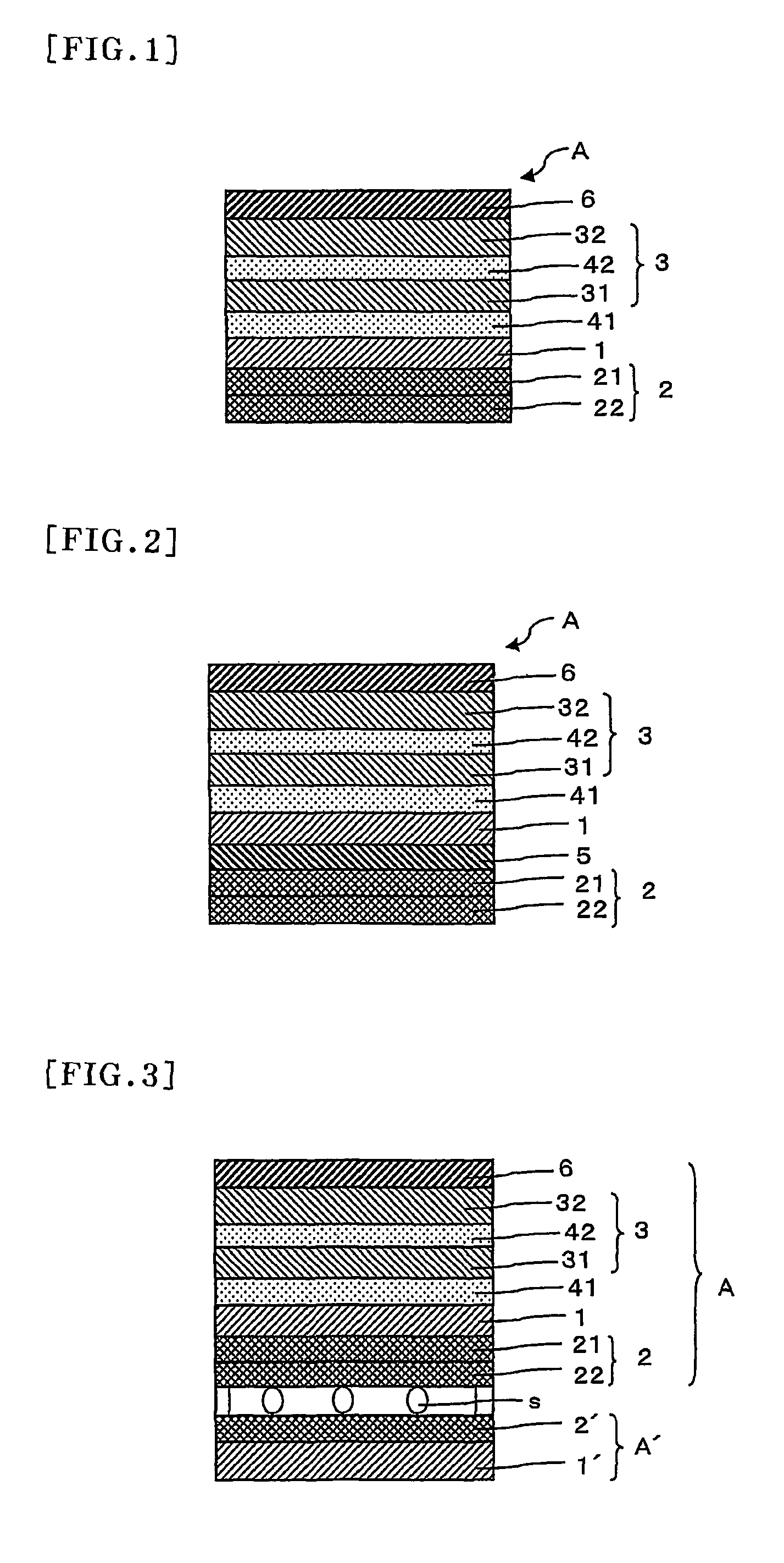
[0081]A 30 nm-thick undercoat layer (transparent dielectric thin film) of a thermosetting resin (with a light refractive index n of 1.54) composed of a melamine resin, an alkyd resin and an organosilane condensate (2:2:1 in weight ratio) was formed on one side of a film substrate made of a 25 μm-thick polyethylene terephthalate film (hereinafter referred to as “PET film”).
[0082]A 20 nm-thick first transparent conductive thin film (with a light refractive index of 2.0) of an indium-tin complex oxide was formed on the undercoat layer by a reactive sputtering method using a sintered material composed of 95% indium oxide and 6% tin oxide in a 0.4 Pa atmosphere composed of 95% by volume of argon gas and 5% by volume of oxygen gas.
[0083]A 5 nm-thick second transparent conductive thin film of an indium-tin complex oxide was formed on the first transparent conductive thin film by a reactive sputtering method using a sintered material composed of...
example 2
[0089]A transparent conductive laminated plate was prepared using the process of example 1, except that a sintered material composed of 97% by weight of indium oxide and 3% by weight of tin oxide was used instead in the process of forming the first transparent conductive thin film described in the section “Formation of Transparent Conductive Thin Films” of example 1.
example 3
[0090]A transparent conductive laminated plate was prepared using the process of example 1, except that in the process of forming the transparent conductive films described in example 1, a 200 nm-thick undercoat layer of a thermosetting resin (with a light refractive index n of 1.54) composed of a melamine resin, an alkyd resin and an organosilane condensate (2:2:1 in weight ratio) was formed instead, and then a 30 nm-thick SiO2 film (with a light refractive index of 1.46) was formed by a silica coating method including the steps of diluting a silica sol (Colcoat P, manufactured by Colcoat Co., Ltd.) with ethanol to a solid concentration of 2%, applying the diluted silica sol to the thermosetting resin layer, and then curing it after drying at 150° C. for 2 minutes.
PUM
| Property | Measurement | Unit |
|---|---|---|
| thickness | aaaaa | aaaaa |
| thickness | aaaaa | aaaaa |
| temperature | aaaaa | aaaaa |
Abstract
Description
Claims
Application Information

