

Organic thin-film transistor substrate, its manufacturing method, image display panel, and its manufacturing method
a thin-film transistor and substrate technology, applied in the direction of transistors, thermoelectric devices, semiconductor/solid-state device details, etc., can solve the problem of high manufacturing cost, and achieve the effect of manufacturing steps
- Summary
- Abstract
- Description
- Claims
- Application Information
AI Technical Summary
Benefits of technology
Problems solved by technology
Method used
Image

Examples
first embodiment
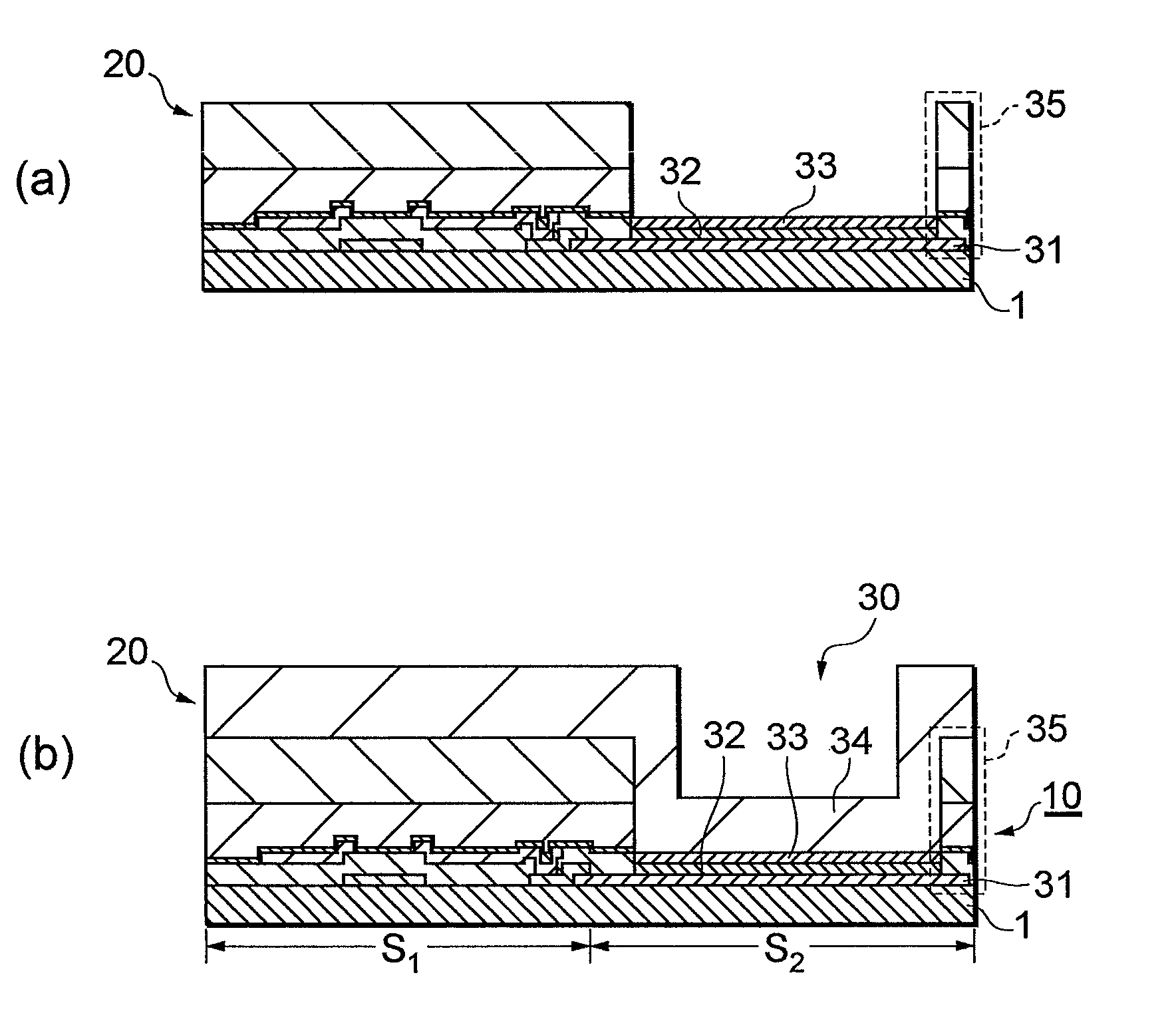
[0040]FIGS. 1 to 4 are diagrams illustrating manufacturing steps of an image display panel in accordance with a first embodiment. In the following description, an explanation will be made of an example in which a bottom-gate organic thin-film transistor including a gate electrode on the substrate side is formed and an organic electroluminescence (EL) element is formed as a light-emitting element.
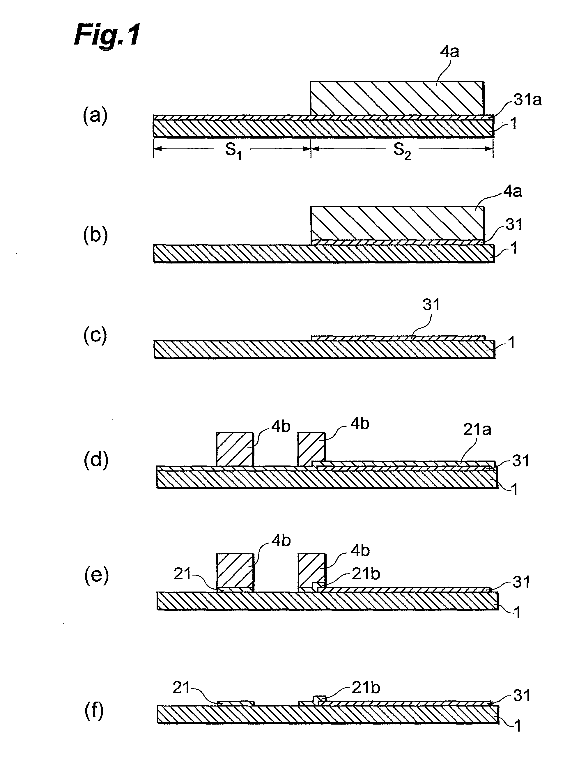
[0041]First, a substrate 1 including a first region S1 and a second region S2 is prepared and an anode (lower electrode) 31 for a light-emitting element 30 is formed in the second region S2 on this substrate 1. Specifically, a conductive film 31a for forming the anode 31 is deposited in the first region S1 and the second region S2 on the substrate 1, for example, and then a resist film 4a is formed on the conductive film 31a of the second region S2 (FIG. 1(a)). Next, using the resist film 4a as a mask, the conductive film 31a in regions in which this resist film 4a is not formed is removed b...
second embodiment
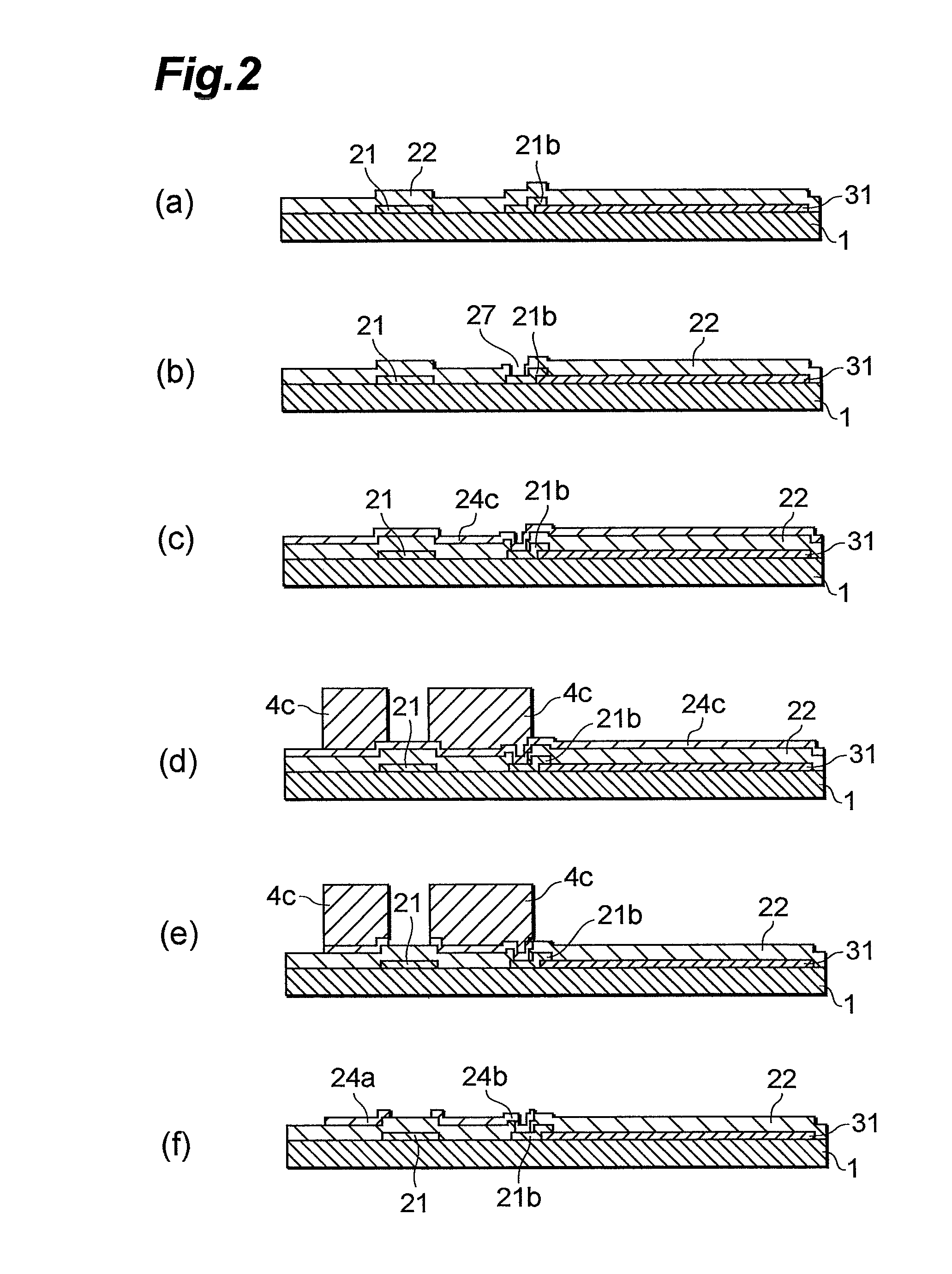
[0094]FIGS. 5 to 8 are diagrams illustrating manufacturing steps of an image display panel in accordance with a second embodiment. In the following description, an explanation will be made of an example in which a top-gate organic thin-film transistor including a gate electrode on an upper portion thereof is formed and an organic EL element is formed as a light-emitting element. Note that the same materials and manufacturing methods can be applied to the same constituent elements as those of the above-described first embodiment and, therefore, the constituent elements will not be explained hereinafter.
[0095]First, on a substrate 1 including a first region S1 and a second region S2, there is formed an anode 31 for a light-emitting element 30 in the second region S2 in the same way as in the first embodiment (FIGS. 5(a) to 5(c)).
[0096]Next, a conductive film 24c to serve as a source electrode 24a and a drain electrode 24b is formed in the first region S1 and the second region S2 on th...
PUM
 Abstract
Description
Claims
Application Information