
Substrate structure and method of manuifacturing the same

a technology of substrate and manufacture method, which is applied in the direction of non-metallic protective coating application, transportation and packaging, nuclear engineering, etc., can solve the problems of large resistance in the heat dissipation path of the heating device, time-consuming and difficult mass production, and achieve the effect of reducing manufacturing time and production cost, reducing manufacturing steps, and being suitable for mass production

Inactive Publication Date: 2016-02-18
SUBTRON TECH
View PDF5 Cites 0 Cited by
  • Summary
  • Abstract
  • Description
  • Claims
  • Application Information

AI Technical Summary

Benefits of technology

The invention is a substrate structure that has a patterned circuit layer embedded within an insulation substrate using a simplified manufacturing process. This reduces production time and cost and makes it suitable for mass production. The patterned circuit layer is located in an intaglio pattern on the insulation substrate, which also reduces the thickness of the substrate. This reduces thermal resistance and enhances heat conduction.

Problems solved by technology

Thereby, the thermal resistance in the heat dissipation path of the heating device is larger, and the effect of rapid thermal conduction is not achieved.
However, such means all increase the manufacturing steps and are time-consuming and not easy for mass production.

Method used


Image

  • Substrate structure and method of manuifacturing the same
  • Substrate structure and method of manuifacturing the same
  • Substrate structure and method of manuifacturing the same

Examples


Embodiment Construction

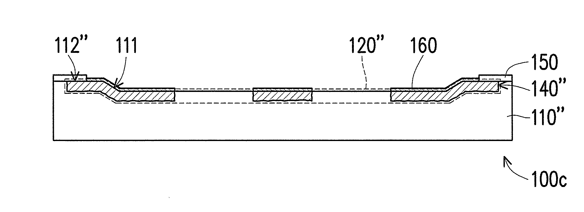
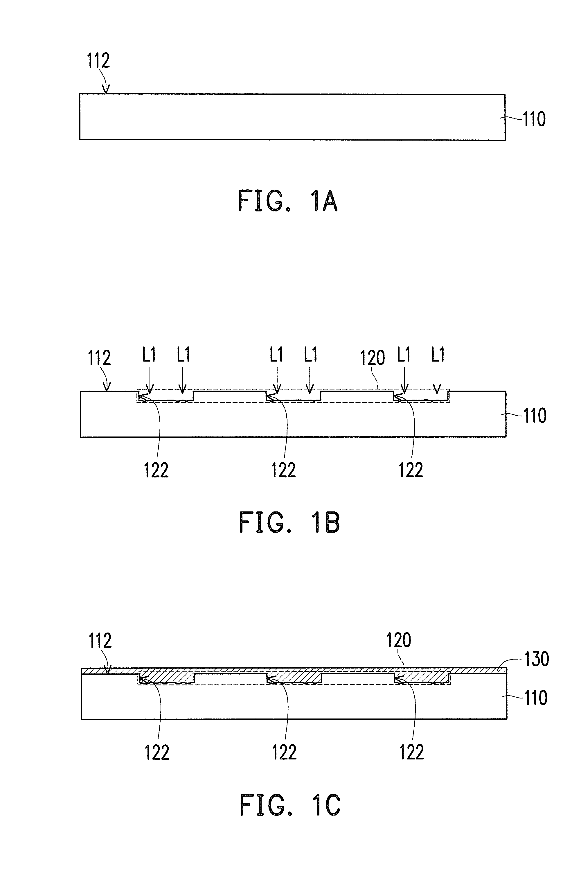
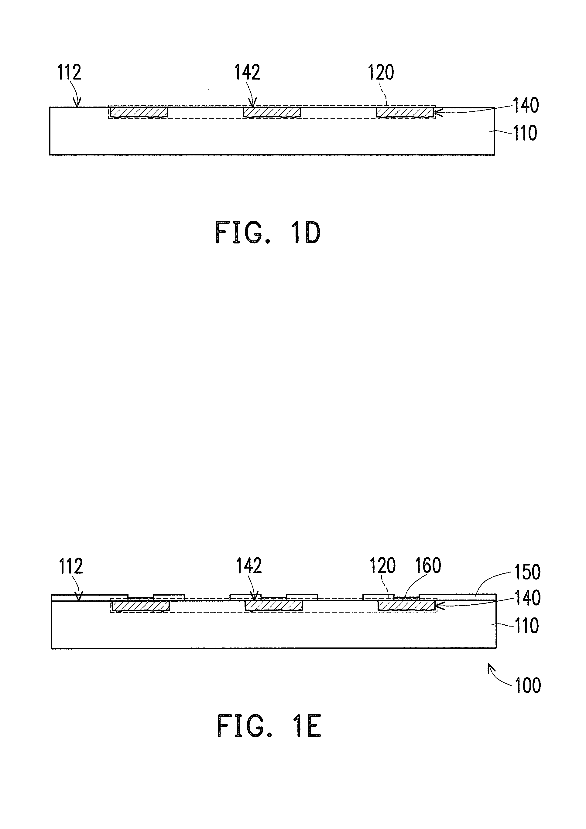
[0033]FIGS. 1A to 1E are schematic cross-sectional views of a method of manufacturing a substrate structure according to an embodiment of the invention. Referring to FIG. 1E, in this embodiment, a substrate structure 100 includes an insulation substrate 110 and a first patterned circuit layer 140. The insulation substrate 110 has an upper surface 112 and a first intaglio pattern 120 situated on the upper surface 112. The first patterned circuit layer 140 is disposed in the first intaglio pattern 120 and fills up the first intaglio pattern 120, wherein a first surface 142 of the first patterned circuit layer 140 is coplanar with the upper surface 112 of the insulation substrate 110. Furthermore, to protect the first patterned circuit layer 140 effectively, the substrate structure 100 of this embodiment may further include a solder mask 150 and a surface treatment layer 160. The solder mask 150 is disposed on the first patterned circuit layer 140 and exposes a portion of the first pat...


PUM


Abstract

A method of manufacturing a substrate structure is provided. An insulation substrate having an upper surface is provided. A portion of the upper surface of the insulation substrate is irradiated by a first laser beam so as to form a first intaglio pattern. The first laser beam is IR laser beam or fiber laser beam. The first intaglio pattern has a modification surface. A first metal layer is formed on the upper surface of the insulation substrate, and covers the upper surface of the insulation layer and the modification surface of the first intaglio pattern, and fills up the first intaglio pattern. A grinding process is performed on the first metal layer so as to expose the upper surface of the insulation substrate and define a first patterned circuit layer. A first upper surface of the first patterned circuit layer is aligned with the upper surface of the insulation substrate.

Description

CROSS-REFERENCE TO RELATED APPLICATION[0001]This application claims the priority benefit of Taiwan application serial no. 103127636, filed on Aug. 12, 2014. The entirety of the above-mentioned patent application is hereby incorporated by reference herein and made a part of this specification.BACKGROUND OF THE INVENTION[0002]1. Field of the Invention[0003]The invention relates to a substrate structure and a method of manufacturing the same, and more particularly to a substrate structure having more preferable thermal conducting effects and a method of manufacturing the same.[0004]2. Description of Related Art[0005]In general, when manufacturing a circuit layer on an insulation substrate, the circuit layer is usually manufactured on an upper surface of the insulation substrate. Therefore, when a heating device is disposed on the circuit layer, the heat generated by the heating device has to pass through the thickness of the circuit layer and the thickness of the insulation substrate t...

Claims


Application Information

Patent Timeline
Patent Type & Authority Applications(United States)
IPC IPC(8): H05K3/00H05K1/02H05K3/04
CPCH05K3/0029H05K3/045H05K2201/0305H05K2203/025H05K2203/072H05K1/0296H05K1/0209H05K3/28H05K2201/0376H05K2201/098
Inventor TSENG, TZYY-JANGWU, CHIEN-NAN
Owner SUBTRON TECH
Learn More