Electronic parts packaging structure and method of manufacturing the same

a technology of electronic parts and packaging structure, applied in the direction of printed circuit manufacturing, printed circuit non-printed electric component association, basic electric elements, etc., can solve the problem of difficult to form desired resist patterns with good precision, and achieve good precision, small depth of focus in exposure, and elimination of variation in bonded height

Inactive Publication Date: 2005-08-16
SHINKO ELECTRIC IND CO LTD
View PDF12 Cites 13 Cited by
  • Summary
  • Abstract
  • Description
  • Claims
  • Application Information

AI Technical Summary

Benefits of technology

[0014]Accordingly, in the situation that the overlying wiring patterns connected electrically to the electronic parts and the wiring patterns are to be formed on the insulating film, when the resist film is patterned by the photolithography, the underlying insulating film is planarized and thus a depth of focus in exposure can be set small. As a result, the desired overlying wiring patterns can be formed over the electronic parts stably with good precision.
[0015]In addition, differences in level are not generated on the overlying wiring patterns. Therefore, when the bumps of the electronic parts are flip-chip mounted on the overlying wiring patterns, variation in a bonded height can be eliminated. Therefore, reliability of the bonding between the bumps of the electronic parts and the overlying wiring patterns can be improved.
[0016]Further, in the case that the packaging areas of the electronic parts are secured by providing non-forming portions of the wiring pattern simultaneously in the step of forming the wiring patterns, manufacturing steps can be reduced rather than the method of planarizing the insulating film by the polishing in the later step. Thus, a production cost can be reduced.
[0017]Moreover, in one preferred mode of the present invention, when the wiring patterns are formed in areas except the packaging areas after the electronic parts are mounted on the mounted body, the resin film having a tackiness in its uncured state may be employed as the mounted body and then the electronic parts may be adhered onto the uncured resin film. Then, the resin film is cured by the annealing in the later step, and thus the electronic parts are firmly fixed to the resin film. If doing so, the step of forming the adhesive layer on the back surfaces (opposite surfaces to the connection terminal side) of the electronic parts is not required particularly. As a result, a production cost can be reduced.

Problems solved by technology

Therefore, it is possible that it become difficult to form desired resist patterns with good precision.

Method used


Image

  • Electronic parts packaging structure and method of manufacturing the same
  • Electronic parts packaging structure and method of manufacturing the same
  • Electronic parts packaging structure and method of manufacturing the same

Examples


first embodiment

[0031](First Embodiment)

[0032]Next, a method of manufacturing an electronic parts packaging structure according to a first embodiment of the present invention will be explained hereunder. FIG. 2A to FIG. 2N are partial sectional views showing the method of manufacturing the electronic parts packaging structure according to the first embodiment of the present invention.

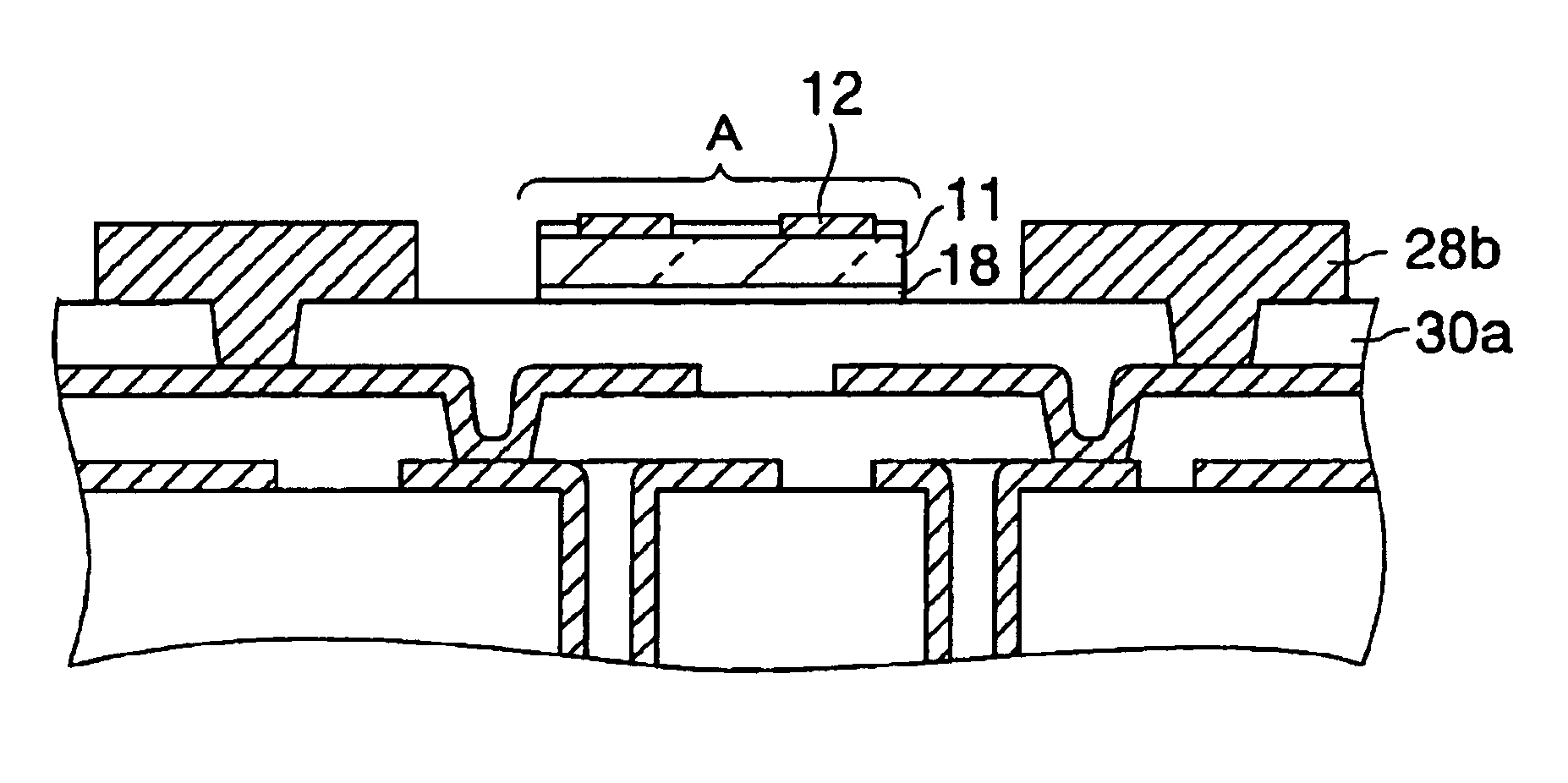
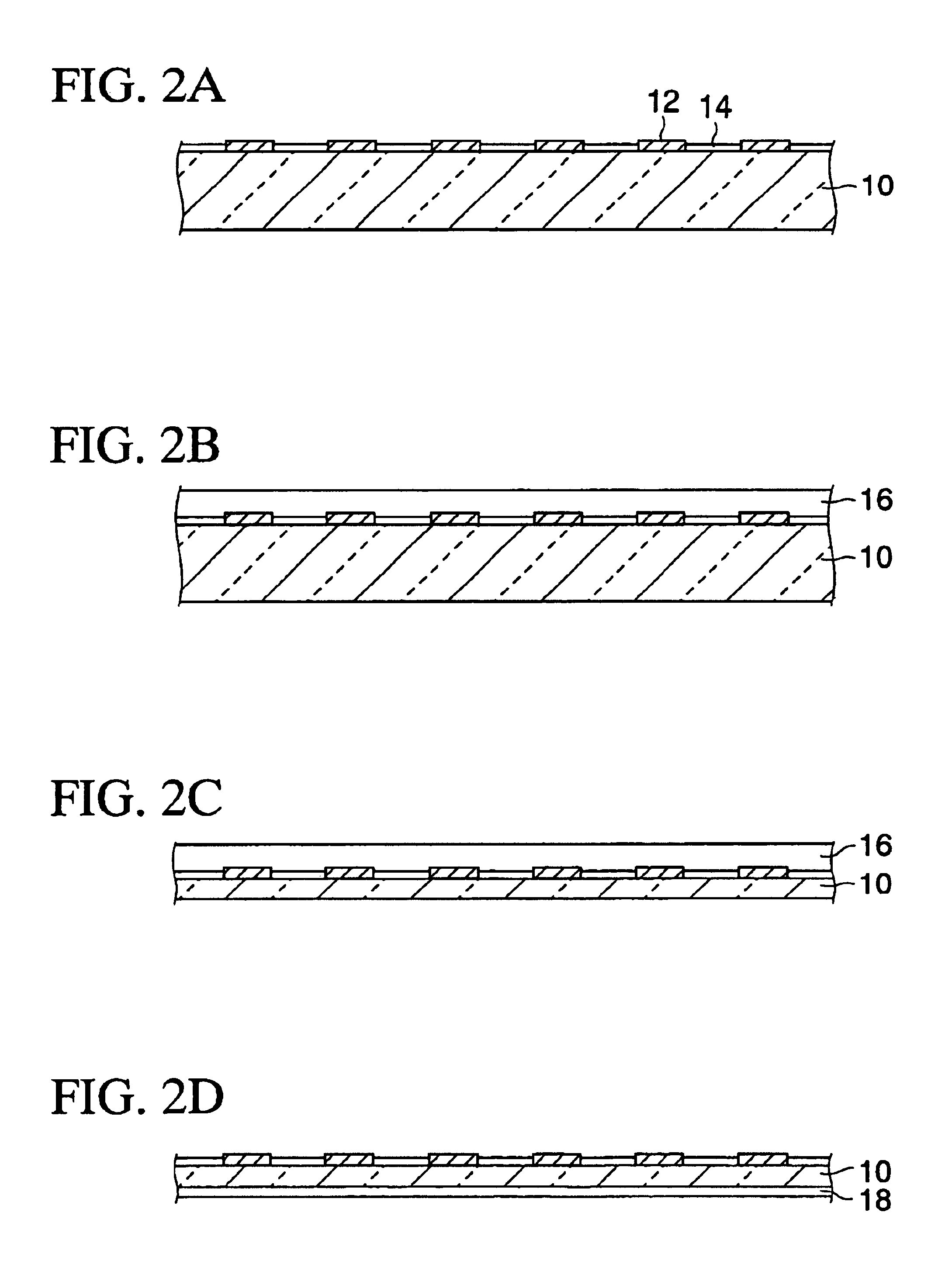
[0033]As shown in FIG. 2A, first a silicon wafer 10 (semiconductor wafer) on which predetermined transistors, multi-layered wirings (not shown), etc. are formed and which has a thickness of about 400 μm is prepared. Connection terminals 12 made of Al, or the like are exposed from an upper surface of the silicon wafer 10. Portions except the connection terminals 12 are covered with a passivation film 14 made of a silicon nitride film, a polyimide resin, or the like.

[0034]Then, as shown in FIG. 2B, mask member 16 is pasted on a surface of the silicon wafer 10 on the connection terminal 12 side (referred to as an element ...

second embodiment

[0074](Second Embodiment)

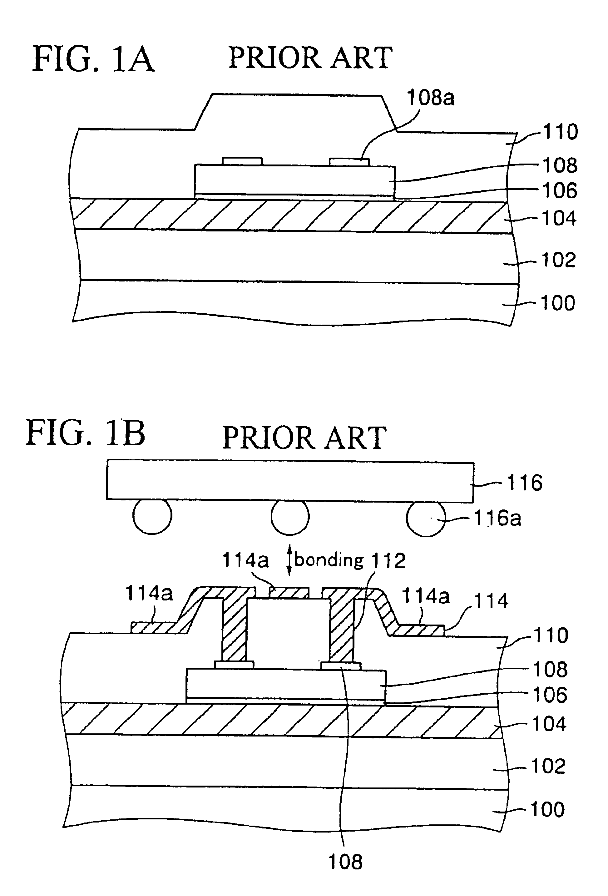
[0075]FIG. 3A to FIG. 3K are partial sectional views showing a method of manufacturing an electronic parts packaging structure according to a second embodiment of the present invention. A different point of the second embodiment from the first embodiment reside in that the semiconductor chips are adhered onto the interlayer insulating film not by forming particularly the die attaching member 18 on the back surfaces of the semiconductor chips 11 but by giving the tackiness to the interlayer insulating film on which the semiconductor chips 11 are mounted. In this case, detailed explanation of the same steps as those in the first embodiment will be omitted herein. Also, in FIG. 3A to FIG. 3K, the same reference symbols are affixed to the same elements as those in FIG. 2A to FIG. 2N, and their explanation will be omitted herein.

[0076]In the method of manufacturing the electronic parts packaging structure according to the second embodiment of the present inventio...

third embodiment

[0093](Third Embodiment)

[0094]FIG. 4A to FIG. 4F are partial sectional views showing a method of manufacturing an electronic parts packaging structure according to a third embodiment of the present invention. A different point of the third embodiment from the first embodiment reside in that the die attaching member is not formed on the back surfaces of the semiconductor chips 11 but a tape containing the adhesive material is employed as the dicing tape, and then such adhesive material is transferred onto the back surfaces of the semiconductor chips 11 when the semiconductor chips 11 are picked up from the dicing tape. In this case, detailed explanation of the same steps as those in the first and second embodiments will be omitted herein. Also, in FIG. 4A to FIG. 4F, the same reference symbols are affixed to the same elements as those in FIG. 2A to FIG. 2N and FIG. 3A to FIG. 3K, and their explanation will be omitted herein.

[0095]In the method of manufacturing the electronic parts pa...


PUM


Abstract

There are provided the steps of forming a wiring pattern in an area except packaging area on a mounted body, the package area in which electronic parts is mounted, mounting the electronic parts in the packaging area of the mounted body to direct a surface of the electronic parts, of which a connection terminal is formed, upward, and forming an insulating film which covers the electronic parts and the wiring pattern.

Description

BACKGROUND OF THE INVENTION[0001]1. Field of the Invention[0002]The present invention relates to an electronic parts packaging structure and a method of manufacturing the same and, more particularly, an electronic parts packaging structure in which semiconductor chips, etc. are mounted on a wiring substrate in a state that they are buried in an insulating film and a method of manufacturing the same.[0003]2. Description of the Related Art[0004]The development of the LSI technology as a key technology to implement multimedia devices is proceeding steadily to a higher speed and a larger capacity of the data transmission. According to this, a higher density of the packaging technology as interfaces between the LSI and electronic devices is also proceeding.[0005]In reply to the request of a further higher density, the multichip package (semiconductor device) in which a plurality of semiconductor chips are laminated three-dimensionally on the substrate and packaged has been developed. As ...

Claims


Application Information

Patent Timeline
Patent Type & Authority Patents(United States)
IPC IPC(8): H01L21/02H01L21/67H01L23/538H01L23/52H01L21/68H01L21/58H05K1/18H05K3/46H01L23/12
CPCH01L21/6835H01L23/5383H01L23/5389H01L24/24H01L24/82H01L24/83H05K1/185H01L24/27H01L24/29H01L21/6836H01L2224/16225H01L2221/68327H01L2221/6834H01L2224/16227H01L2224/24226H01L2224/274H01L2224/82039H01L2224/83191H01L2224/8385H01L2924/01004H01L2924/01005H01L2924/01013H01L2924/01029H01L2924/01033H01L2924/01047H01L2924/01078H01L2924/01079H01L2924/07802H01L2924/19041H01L2924/19043H01L2924/30105H01L2924/3025H05K3/4602H01L2224/2919H01L2924/01006H01L2924/014H01L2924/0665H01L2924/00H01L2924/12042H01L21/50
Inventor SUNOHARA, MASAHIROMURAYAMA, KEIHIGASHI, MITSUTOSHI
Owner SHINKO ELECTRIC IND CO LTD
Why Eureka
Try Eureka