Nitride semiconductor light emitting element

a light-emitting element and nitride technology, applied in the direction of basic electric elements, semiconductor devices, electrical equipment, etc., can solve the problems of insufficient curing of deeper portions, difficult to produce efficient and stable ratio of emission peak intensity, and decrease in luminous efficiency in longer wavelengths. , to achieve the effect of large band gap energy, stable ratio of emission intensity, and large bang gap energy

Active Publication Date: 2011-10-04
NICHIA CORP
View PDF12 Cites 5 Cited by
  • Summary
  • Abstract
  • Description
  • Claims
  • Application Information

AI Technical Summary

Benefits of technology

[0011]As described above, in the cases where a well layer having smaller band gap energy is disposed closer to the p-type semiconductor layer side than a well layer having a larger band gap energy, single peak emission tends to be obtained, and this is considered that emission from the well layer having smaller band gap energy or a well layer which is close to the p-type semiconductor layer is facilitated, when an active layer is nitride semiconductor, especially nitride gallium based compound semiconductor. On the other hand, it is considered that in the cases where the well layer having smaller band gap energy is disposed closer to the n-type semiconductor layer side than the well layer having a bigger band gap energy, the electron confinement effect is degraded due to its small band gap energy, and the luminous efficiency is decreased, resulting in an element in which the ratio of emission peak intensity tends to fluctuate.
[0016]In a nitride semiconductor light emitting element according to the present invention, the outermost well layers are the second well layers having a larger band gap energy, and a first well layer having a smaller band gap energy is disposed at an inner side thereof. With this arrangement, the second well layer having a large band gap energy can emit light, and electron confinement effect can also be obtained by interposing the first well layer between the second well layers which have a larger bang gap energy. Thus, an emission spectrum having two peaks with stable ratio of emission intensity can be obtained.

Problems solved by technology

However, in the cases where a semiconductor light emitting element is used in a ultraviolet irradiating apparatus for curing a material, with a larger thickness of the irradiated material, insufficient curing of a deeper portions may result.
However, in the semiconductor light emitting element in which well layers of different emission wavelengths are simply stacked in order of wavelength, it is difficult to produce an efficient and stable ratio of emission peak intensity.
For example, in a case where a well layer of longer wavelength emission having a smaller band gap energy is disposed closer to the n-type semiconductor layer side than a well layer of shorter wavelength emission having a larger band gap energy, the luminous efficiency in longer wavelength decreases, so that stable ratio of emission peak intensity is difficult to obtain.
Such a nitride semiconductor light emitting element having unstable ratio of emission peak intensity is unsuitable as the light source for curing a resin or an ink.

Method used


Image

  • Nitride semiconductor light emitting element
  • Nitride semiconductor light emitting element
  • Nitride semiconductor light emitting element

Examples


embodiment 1

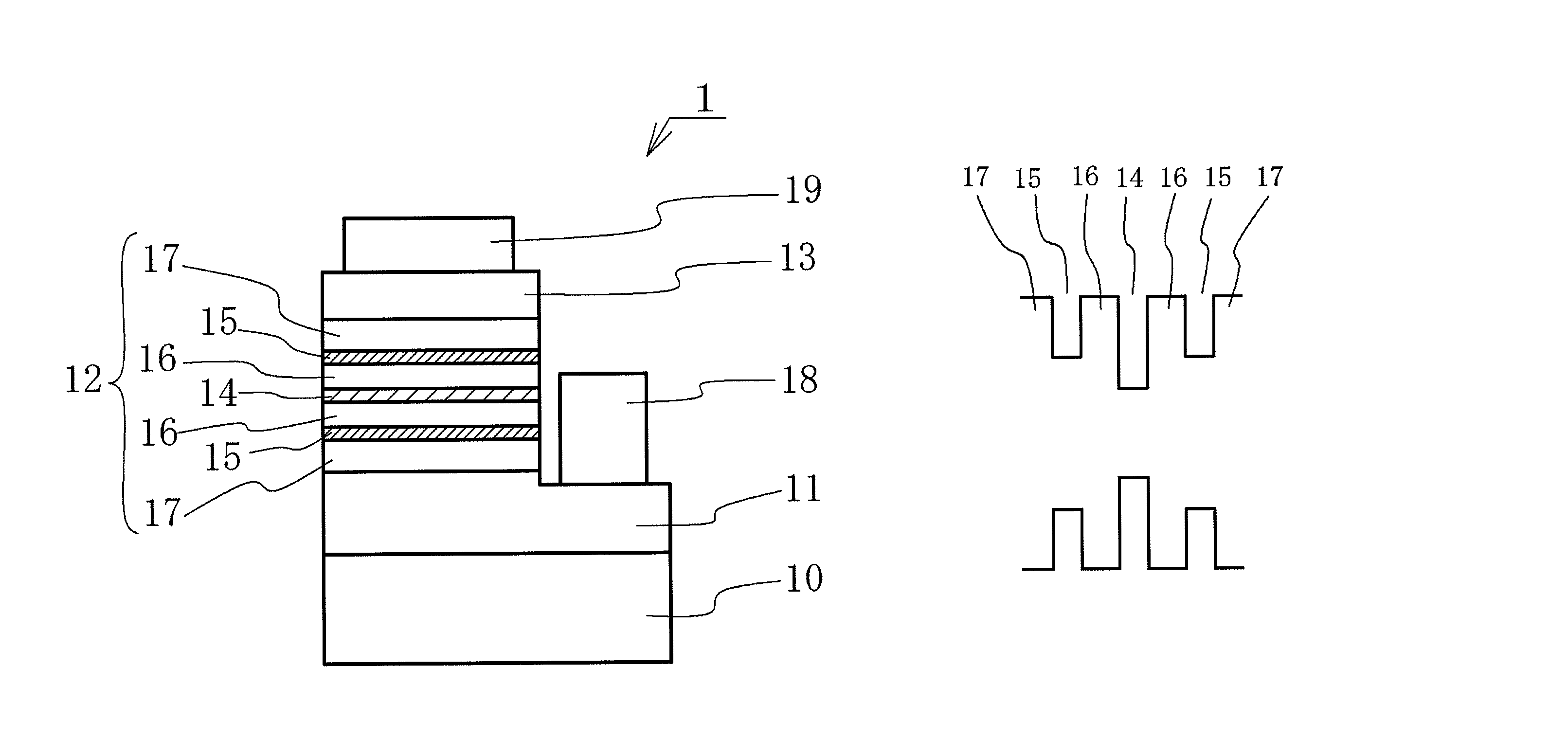
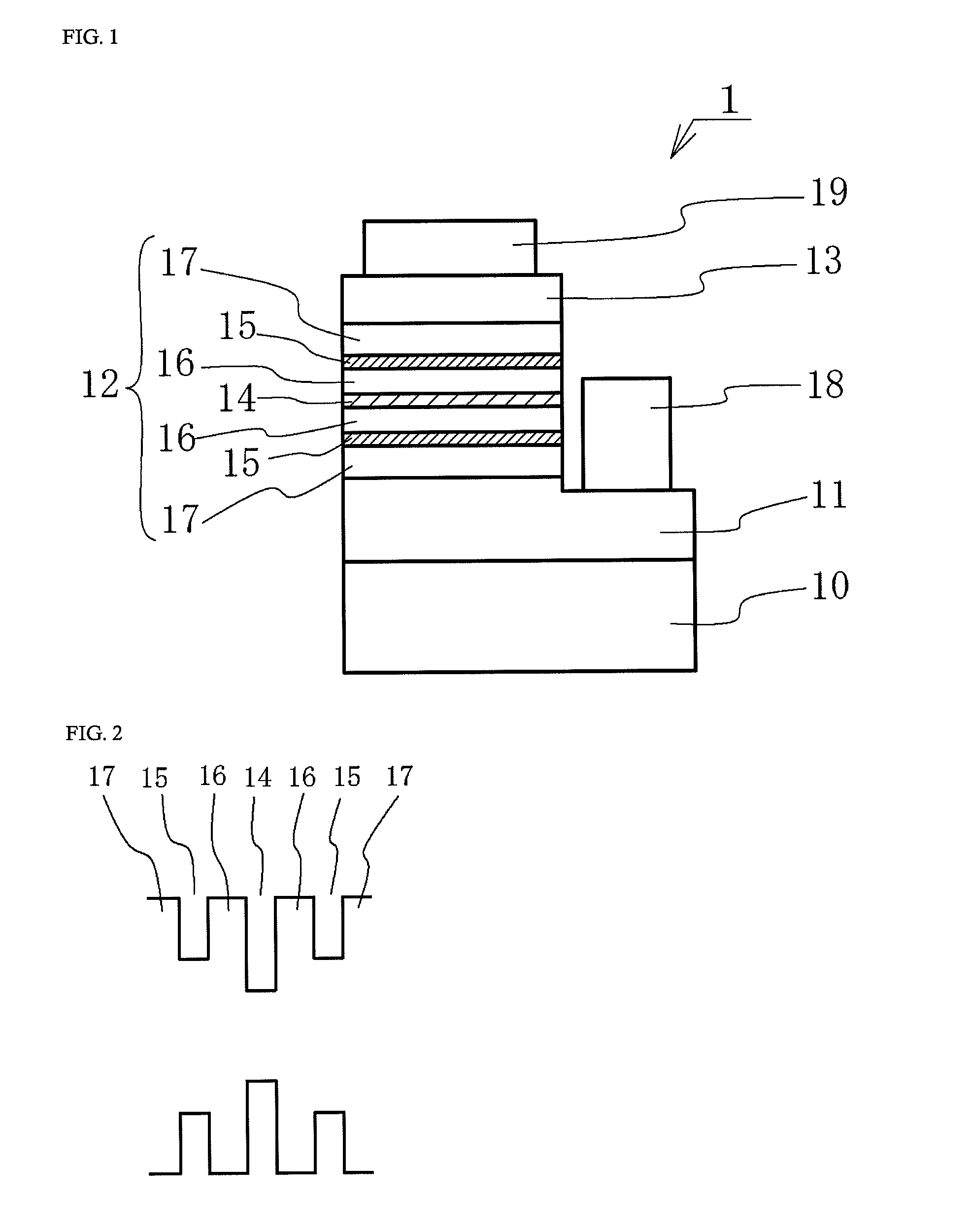
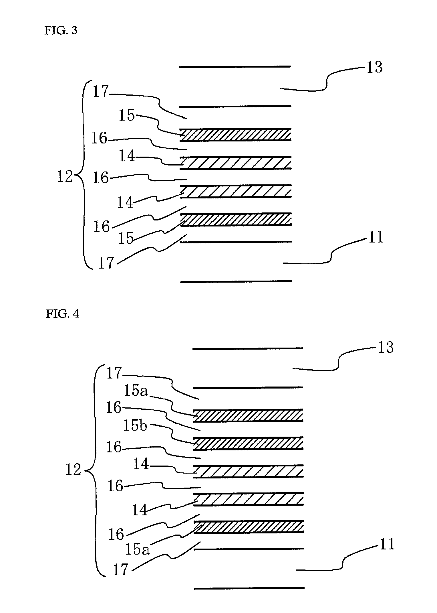
[0033]FIG. 1 is a cross-sectional view schematically showing a structure of a nitride semiconductor light emitting element according to Embodiment 1 of the present invention. The nitride semiconductor light emitting element 1 includes an n-type nitride semiconductor layer 11, an active layer 12, and a p-type nitride semiconductor layer 13, stacked in this order on a substrate 10. An n-electrode18 is disposed on a portion of the n-type semiconductor layer 11 which is exposed by removing a portion of the p-type nitride semiconductor layer 13, and a p-electrode 19 is disposed on the p-type nitride semiconductor layer 13. The active layer 12 contains a first well layer 14 and second well layers 15 interposing the first well layer 14 therebetween, and barrier layers 16, 17. One second well layer 15 is disposed at respective outermost sides among the well layer, that is, at the closest side to the n-type nitride semiconductor layer 11 and at the closest side to the p-type nitride semicond...

embodiment 2

[0056]FIG. 6 is a cross-sectional view schematically showing a structure of a nitride semiconductor light emitting element according to Embodiment 2 of the present invention. The nitride semiconductor light emitting element 2 has a stacked layer structure in which, the p-type nitride semiconductor layer 23, the active layer 22, the n-type nitride semiconductor layer 21 are stacked in this order via the conductive bonding layer 201 on the supporting substrate 200, and the n-electrode 28 and the p-electrodes 29 are respectively disposed on the opposite sides of the stacked layer structure. As described above, the nitride semiconductor light emitting element 2 of Embodiment 2 has a counter electrode structure in which the p-electrode 29 and the n-electrode 28 are disposed on the respective opposing sides of the stacked layer structure, and the p-electrode 29 side is bonded to the supporting substrate 200. Substantially the same members as in Embodiment 1 can be used as the members comm...

example 1

[0061]The nitride semiconductor light emitting element according to Example 1 includes, as shown in FIG. 6, a stacked layer structure in which the p-type nitride semiconductor layer 23, the active layer 22, and the n-type nitride semiconductor layer 21 are stacked via the conductive bonding layer 201 on the supporting substrate 200 made of an alloy of Cu and W, and the p-electrode 29 is disposed at the p-type nitride semiconductor layer 23 side and the n-electrode 28 is disposed at the n-type nitride semiconductor layer 21 side.

[0062]The nitride semiconductor light emitting element 2 can be formed as shown below. First, using a substrate made of sapphire (C-plane) as the growth substrate, a buffer layer made of GaN with a thickness of 200 angstromes and an under layer made of undoped GaN with a thickness of 4 □m are grown in this order on the substrate. Next, as the n-type nitride semiconductor layer 21, an n-type contact layer of Si-doped Al0.07Ga0.93N is grown to a thickness of ab...


PUM


Abstract

Provided is a nitride semiconductor light emitting element capable of producing an emission spectrum having two peaks with stable ratio of emission peak intensity. The nitride semiconductor light emitting 1 comprises an active layer 12 disposed between an n-type nitride semiconductor layer 11 and a p-type nitride semiconductor layer 13. The active layer 12 comprises a first well layer 14, second well layers 15 interposing the first well layer 14 and disposed at outermost sides among the well layers, and barrier layers 16, 17 disposed between each of the well layers. The second well layer 15 comprises a nitride semiconductor having a larger band gap energy than the band gap energy of a nitride semiconductor constituting the first well layer 14, and the nitride semiconductor light emitting element 1 has peaks in the emission spectrum respectively corresponding to the first well layer 14 and the second well layer 15.

Description

CROSS-REFERENCE TO RELATED APPLICATIONS[0001]The present application claims priority under 35 U.S.C. §119 to Japanese Patent Application No. 2008-268204, filed in Japan on Oct. 17, 2008, the contents of which are incorporated hereinto by reference.BACKGROUND OF THE INVENTION[0002]1. Field of the Invention[0003]The present invention relates to a nitride semiconductor light emitting element, in particular, a nitride semiconductor light emitting element having a plurality of peaks in its emission spectrum.[0004]2. Discussion of the Related Art[0005]In recent years, semiconductor light emitting elements capable of emitting light in the ultraviolet region have been put into practical use, which are also used in an exposure apparatus, a disinfection apparatus, and the like. However, in the cases where a semiconductor light emitting element is used in a ultraviolet irradiating apparatus for curing a material, with a larger thickness of the irradiated material, insufficient curing of a deep...

Claims


Application Information

Patent Timeline
Patent Type & Authority Patents(United States)
IPC IPC(8): H01L33/00
CPCH01L33/06H01L33/08H01L33/32
Inventor UBAHARA, NOBUHIRO
Owner NICHIA CORP
Why Eureka
Try Eureka