Scan driving circuit and organic light emitting display using the same

a driving circuit and organic technology, applied in the direction of instruments, static indicating devices, electroluminescent light sources, etc., can solve the problems of difficult mounting a conventional scan driver or emission control driver on a panel, difficult to drive a conventional emission control driver at a high speed, and the power consumption of conventional scan driver or emission control driver composed of pmos transistors and nmos transistors is relatively high, so as to achieve the effect of low power consumption

Active Publication Date: 2011-10-04
SAMSUNG DISPLAY CO LTD
View PDF34 Cites 23 Cited by
  • Summary
  • Abstract
  • Description
  • Claims
  • Application Information

AI Technical Summary

Benefits of technology

[0011]It is therefore a feature of an embodiment of the present invention to provide a scan driving circuit that minimizes or reduces power consumption relative to conventional scan driving circuits.
[0014]It is therefore a separate feature of an embodiment of the present invention to provide a scan driving circuit that includes a second scan driver having a low amount of power consumption.
[0015]It is therefore a separate feature of an embodiment of the present invention to provide a scan driving circuit that eliminates a path through which static current may flow.

Problems solved by technology

However, it is difficult to mount a conventional scan driver or emission control driver on a panel because the conventional scan driver or emission control driver is composed of PMOS transistors and NMOS transistors.
Also, it is difficult to drive a conventional emission control driver at a high speed because the conventional emission control driver generates an output signal per at least one cycle of a clock signal.
Also, the conventional scan driver or emission control driver composed of the PMOS transistors and the NMOS transistors has a relatively high level of power consumption because a predetermined static current flows when an output signal is generated.

Method used


Image

  • Scan driving circuit and organic light emitting display using the same
  • Scan driving circuit and organic light emitting display using the same
  • Scan driving circuit and organic light emitting display using the same

Examples


Embodiment Construction

[0040]Korean Patent Application No. 10-2006-0031636, filed on Apr. 6, 2006, in the Korean Intellectual Property Office, and entitled: “Scan Driving Circuit and Organic Light Emitting Display Using the Same,” is incorporated by reference herein in its entirety.

[0041]The present invention will now be described more fully hereinafter with reference to the accompanying drawings, in which exemplary embodiments of the invention are illustrated. The invention may, however, be embodied in different forms and should not be construed as limited to the embodiments set forth herein. Rather, these embodiments are provided so that this disclosure will be thorough and complete, and will fully convey the scope of the invention to those skilled in the art.

[0042]In the figures, the dimensions of layers and regions may be exaggerated for clarity of illustration. Like reference numerals refer to like elements throughout.

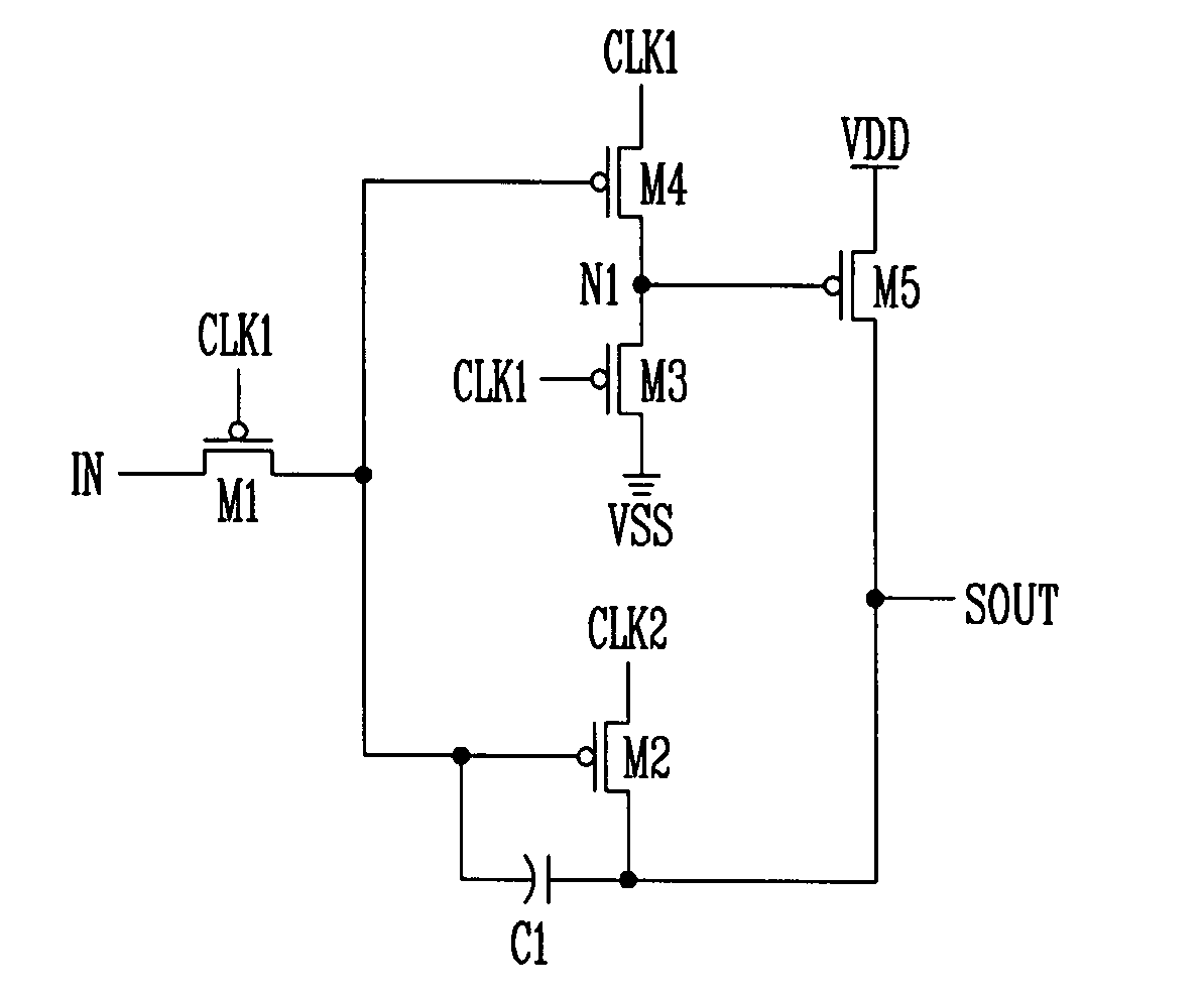
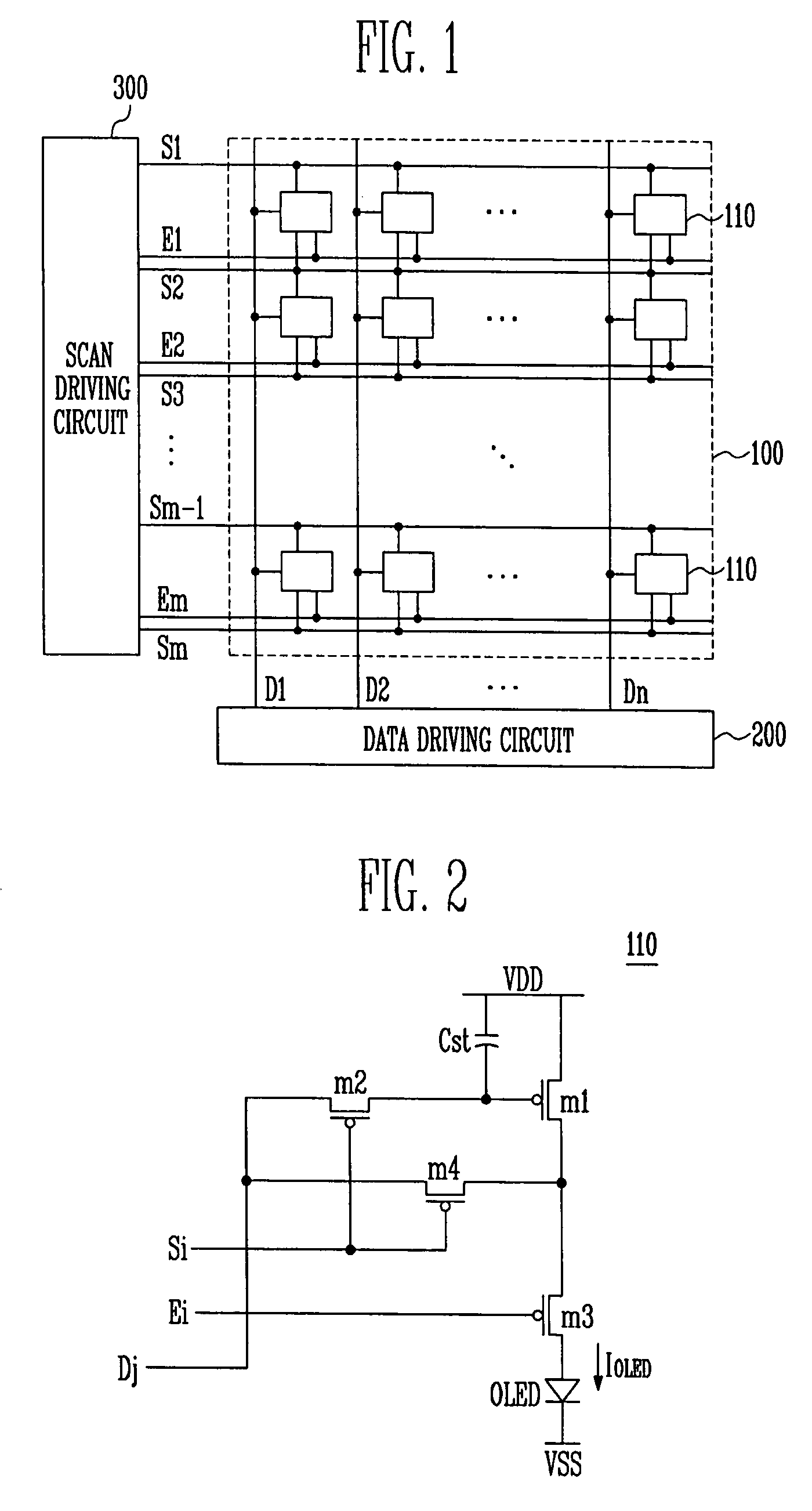
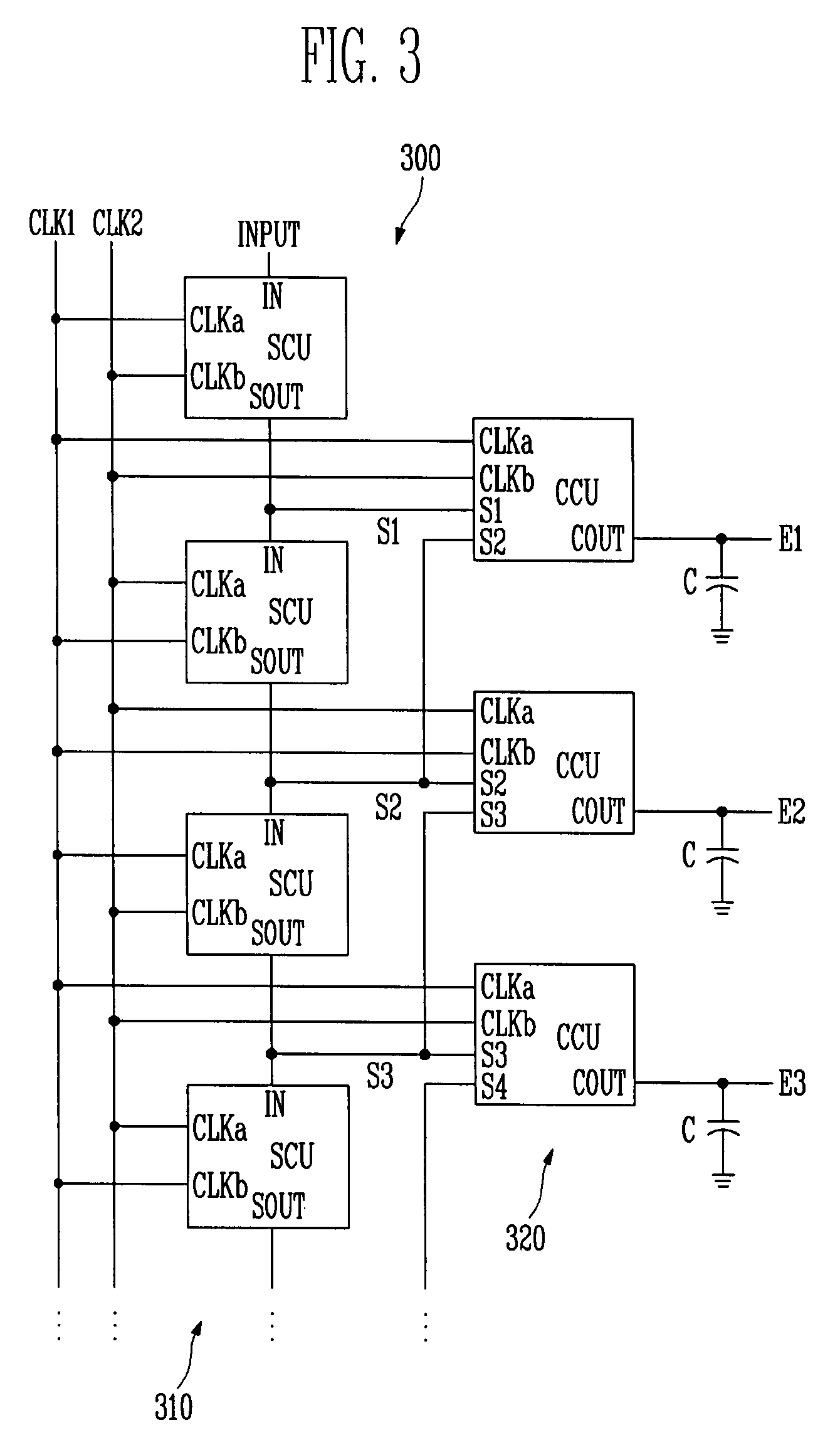
[0043]FIG. 1 illustrates a schematic view of an exemplary organic light emitting di...


PUM


Abstract

A scan driving circuit includes a first scan driver including a plurality of first units, the first units receiving an input signal or an output voltage of a previous first unit and first and second clock signals to output a scan signal, and a second scan driver having a plurality of second units, the second units receiving a plurality of scan signals output from respective ones of the first units, and at least one of the first and second clock signals, and outputting an emission control signal.

Description

BACKGROUND OF THE INVENTION[0001]1. Field of the Invention[0002]The present invention relates to an organic light emitting display. More specifically, the present invention relates to a scan driving circuit employable in a current driven type organic light emitting display.[0003]2. Description of the Related Art[0004]Various types of flat panel displays are being developed. Flat panel display devices are more commonly replacing cathode ray tubes (CRTs) because flat panel display devices may be made to be thinner, have less volume, and / or be lighter than (CRTs). Flat panel displays include, e.g., a liquid crystal display (LCD), a field emission display (FED), a plasma display panel (PDP) and an organic light emitting display (OLED), etc.[0005]Amongst the flat panel displays, organic light emitting displays generally display an image using an organic light emitting diode (OLED) that generates light by the recombination of an electron and a hole. Such an organic light emitting display ...

Claims


Application Information

Patent Timeline
Patent Type & Authority Patents(United States)
IPC IPC(8): G09G3/30H05B44/00
CPCG09G3/325G09G3/3266G11C19/184G09G3/20G09G2300/0842G09G2310/0286G09G2330/021G09G3/30
Inventor SHIN, DONG YONG
Owner SAMSUNG DISPLAY CO LTD
Why Eureka
Try Eureka