Check patentability & draft patents in minutes with Patsnap Eureka AI!

Active matrix organic light emitting diode panel

a technology of organic light and diodes, applied in the direction of instruments, static indicating devices, etc., can solve the problems of improving production cost and providing only limited current idata

Active Publication Date: 2011-10-18
N SPINE INC +2
View PDF9 Cites 2 Cited by
  • Summary
  • Abstract
  • Description
  • Claims
  • Application Information

AI Technical Summary

Benefits of technology

This solution enables the AMOLED panel to provide a range of currents, from the smallest to the largest, effectively driving AMOLED pixels with increased luminance without the need for larger data driving units, thus reducing production costs.

Problems solved by technology

However, the above data driving unit 12 can provide only a limited current IData.
If a larger current is to be required, the area of the data driving unit 12 has to be increased, thereby improving production cost.

Method used


Image

  • Active matrix organic light emitting diode panel
  • Active matrix organic light emitting diode panel
  • Active matrix organic light emitting diode panel

Examples


Embodiment Construction

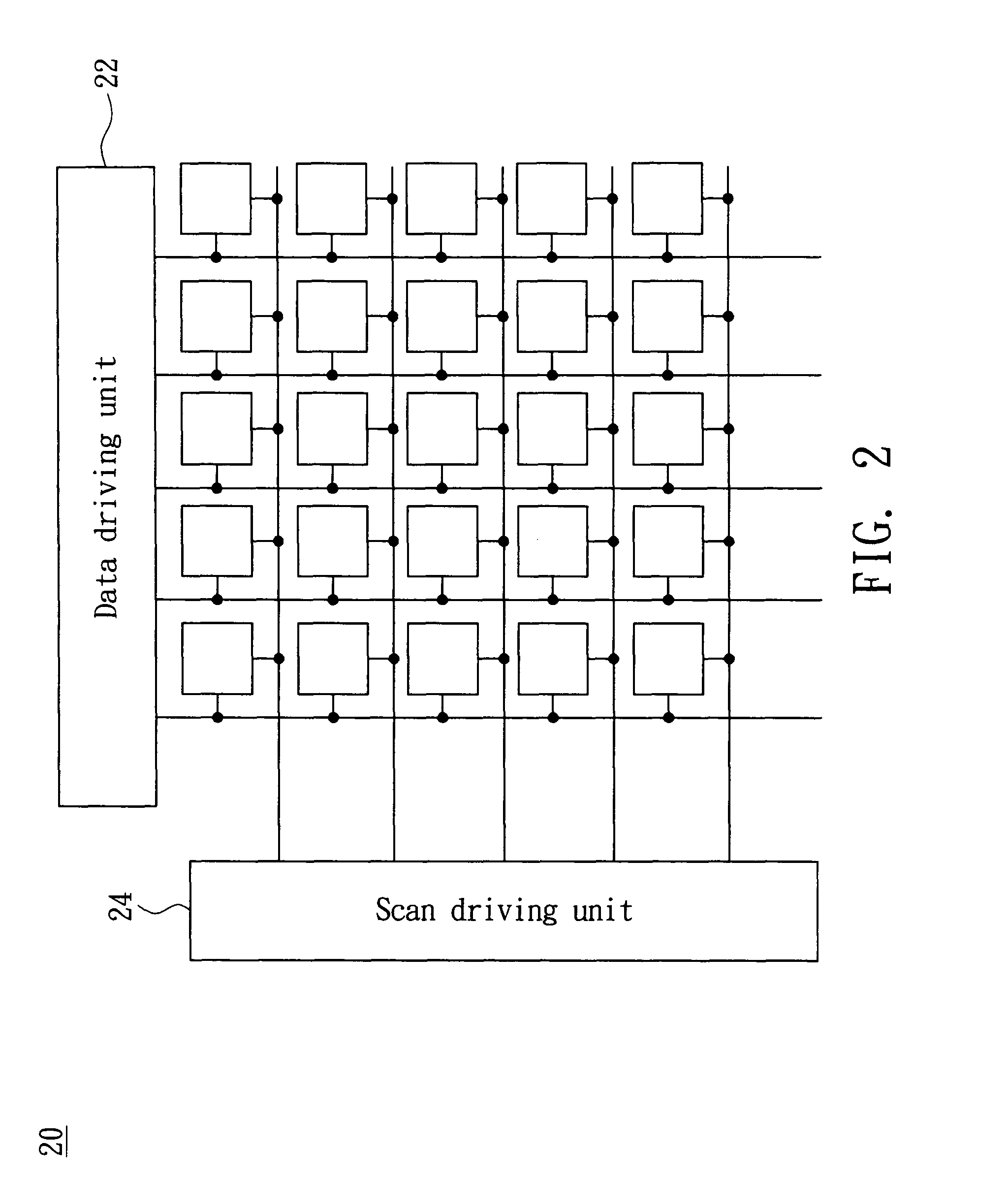
[0015]The invention uses (N+1) mirror output circuits to provide a larger current for driving pixels. Referring to FIG. 2, a function block diagram of an AMOLED pixel driving circuit according to a preferred embodiment of the invention is shown. In the AMOLED pixel driving circuit 20, a data driving unit 22 and a scan driving unit 24 are respectively used to control AMOLEDs in a certain column and row of pixels

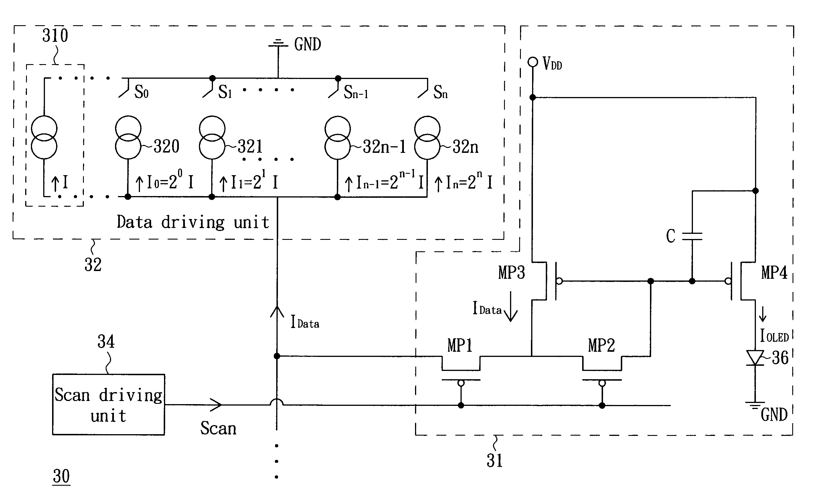
[0016]Referring to FIG. 3, a schematic diagram of an AMOLED panel according to the preferred embodiment of the invention is shown. An AMOLED panel 30 includes an AMOLED pixel unit 31, a data driving unit 32 and a scan driving unit 34. The AMOLED pixel unit 31 includes an AMOLED 36, a first switch element MP1, a second switch element MP2, a third switch element MP3, a fourth switch element MP4 and an energy storage element C. For example, the switch elements MP1˜MP4 are implemented by p-type metal oxide semiconductor (PMOS) transistors and the energy storage element is a capaci...


PUM


Abstract

An AMOLED panel includes an AMOLED pixel unit, a scan driving unit and a data driving unit. The scan driving unit is coupled to the AMOLED pixel unit. The data driving unit is coupled to the AMOLED pixel unit and a voltage source. The data driving unit comprises a reference current source circuit, (N+1) mirror output circuits and (N+1) switch elements. The reference current source circuit is for providing a reference current. (N+1) mirror output circuits are coupled to the reference current source circuits for outputting (N+1) corresponding data currents to the AMOLED pixel unit, wherein N is a positive integer. The m-th data current of the (N+1) data currents is 2m times of the reference current, and m is an integer 0˜N. The switch elements are disposed in correspondence with the mirror output circuits for controlling the data currents to be outputted to the AMOLED pixel unit.

Description

[0001]This application claims the benefit of Taiwan application Serial No. 95116424, filed May 9, 2006, the subject matter of which is incorporated herein by reference.BACKGROUND OF THE INVENTION[0002]1. Field of the Invention[0003]The invention relates in general to an active matrix organic light emitting diode (AMOLED) panel, and more particularly to an AMOLED panel driven by a large current.[0004]2. Description of the Related Art[0005]Normally, in an AMOLED display, images are displayed by a large number of pixels on the AMOLED panel. Each pixel of the AMOLED panel is controlled according to a data signal so as to display the required luminance.[0006]Referring to FIG. 1, a circuit diagram of a conventional AMOLED panel is shown. In an AMOLED panel 10, during a writing time period, a scan signal Scan outputted by a scan driving unit 14 turns on transistors T1 and T2 in the AMOLED pixel unit 11. Due to a current IData of the data driving unit 12, the same current IData is generated...

Claims


Application Information

Patent Timeline
Patent Type & Authority Patents(United States)
IPC IPC(8): G09G3/32
CPCG09G3/3241G09G3/3283G09G2300/0465G09G2300/0842
Inventor HUANG, JIUNN-YAUYEN, CHENG-CHI
Owner N SPINE INC
Features
  • R&D
  • Intellectual Property
  • Life Sciences
  • Materials
  • Tech Scout
  • Unparalleled Data Quality
  • Higher Quality Content
  • 60% Fewer Hallucinations
Learn More