Shift register circuit

a technology of shift register and drive capability, which is applied in the direction of information storage, static storage, digital storage, etc., can solve the problems of hindering the high resolution of display apparatuses, reducing the drive capability of first transistors, and unable to achieve the maximum pre-charge level of the first node, etc., to achieve the effect of suppressing the decrease of drive capability

Active Publication Date: 2011-10-18
TRIVALE TECH
View PDF34 Cites 15 Cited by
  • Summary
  • Abstract
  • Description
  • Claims
  • Application Information

AI Technical Summary

Benefits of technology

[0014]It is the object of the present invention to provide a shift register circuit capable of suppressing a decrease in a drive capability when a frequency of a clock signal increases.
[0016]The third transistor of which control electrode (the third node) is boosted operates to charge (pre-charge) the first node, so that the first node can be sufficiently pre-charged even when the frequency of the clock signal increases and a pulse width of a signal input to the input terminal becomes narrow. In other words, it is possible to prevent the decrease of the drive capability of the first transistor. Furthermore, the third transistor operates in the non-saturated region, so that a loss corresponding to the threshold voltage thereof does not occur, and the first node can be pre-charged to a higher level than ever before. Therefore, the drive capability of the first transistor improves.

Problems solved by technology

However, when the frequency of the clock signal increases, and a pulse width of the input signal (the output signal of the unit shift register of the preceding stage) becomes narrow, it is difficult for the first node to attain the maximum pre-charge level (VDD−Vth).
Therefore, when the frequency of the clock signal increases, the first node cannot be sufficiently pre-charged, which brings about a decrease in the drive capability of the first transistor.
In particular, the gate line driving circuit has a problem in that it is necessary to activate a gate line by charging it rapidly using the output signal of the unit shift register, thus requiring the first transistor to have a high drive capability.
In other words, there is a problem in that it is difficult to cause the gate line driving circuit to operate faster by increasing the frequency of the clock signal, which hinders a display apparatus from achieving a high resolution.

Method used


Image

  • Shift register circuit
  • Shift register circuit
  • Shift register circuit

Examples


first embodiment

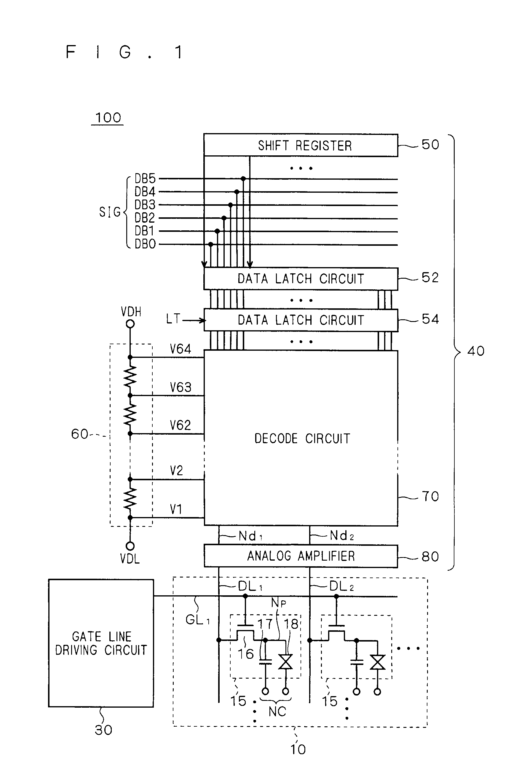
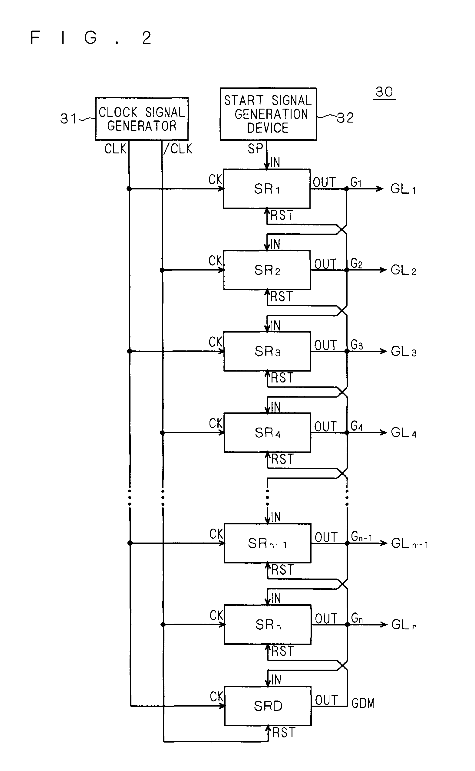
[0066]FIG. 1 is a schematic block diagram showing a configuration of a display apparatus according to the first embodiment of the present invention. In FIG. 1, an entire configuration of a liquid crystal display apparatus 100 is shown as a representative example of the display apparatus. It should be noted that a gate line driving circuit according to the present invention is not limited to application to a liquid crystal display apparatus, and can be widely applied to electro-optic apparatuses such as electroluminescence (EL), organic EL, plasma display, electronic paper, and image sensor. The liquid crystal display apparatus 100 includes a liquid crystal array unit 10, a gate line driving circuit (scanning line driving circuit) 30, and a source driver 40. As will be clear from the following description, a shift register according to the embodiments of the present invention is arranged in the gate line driving circuit 30.

[0067]The liquid crystal array unit 10 includes a plurality o...

second embodiment

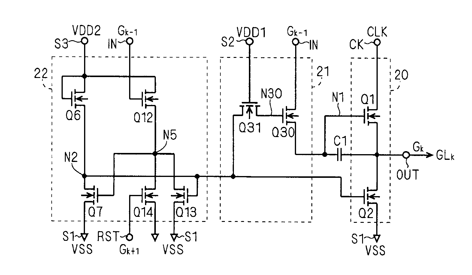
[0186]FIG. 12 is a circuit diagram showing a unit shift register SRk according to the second embodiment. This unit shift register SRk has, in addition to the circuit of FIG. 3, a transistor Q15 connected between the gate of the transistor Q8 and the node N2 (the gate of the transistor Q8 is separated from the second power supply terminal S2) and a transistor Q16 connected between the node N3 and the input terminal IN. The gate of the transistor Q15 is connected to the second power supply terminal S2, and the gate of the transistor Q16 is connected to the node N1. A node connected to the gate of the transistor Q8 is defined as “node N6.”

[0187]In the circuit of FIG. 12, the input terminal IN is connected to the source of the transistor Q16, which means that the output signal of preceding stage Gk−1 is supplied thereto, but the clock signal / CLK having the same phase as the output signal of preceding stage Gk−1 may be supplied instead.

[0188]FIG. 13 is a timing chart for illustrating op...

fourth embodiment

[0257]In the fourth embodiment, the present invention is applied to a shift register which can change a shift direction of a signal. The gate line driving circuit 30 configured with such shift register can scan in both directions.

[0258]FIG. 19 is a circuit diagram showing the unit shift register SRk according to the fourth embodiment. The unit shift register SRk is based on the circuit of FIG. 3 but has a switching circuit 24 for switching a shift direction of a signal.

[0259]In the circuit of FIG. 3, the output signal of preceding stage Gk−1 is input to only one of the current electrodes of the transistor Q8 (input terminal IN), and the output signal of subsequent stage Gk+1 is input to only the gate of the transistor Q4 (reset terminal RST). In contrast, the switching circuit 24 of FIG. 19 can switch the two signals in accordance with the levels of the first and second voltage signals Vn and Vr.

[0260]As shown in FIG. 19, the switching circuit 24 includes transistors Q25r, Q25n, Q26...


PUM


Abstract

A shift register circuit is provided that can suppress a decrease in a drive capability when a frequency of a clock signal increases. A unit shift register includes a first transistor for supplying a clock signal to an output terminal, a pull-up driving circuit for driving the first transistor, a second transistor for discharging the output terminal, and a pull-down driving circuit for driving the second transistor. In the pull-up driving circuit, the gate of a third transistor charging the gate of the first transistor is charged in accordance with activation of an output signal of preceding stage, and the potential at the gate of the third transistor is increased with a capacitive element. As a result, the third transistor operates in the non-saturated region.

Description

BACKGROUND OF THE INVENTION[0001]1. Field of the Invention[0002]The present invention relates to a scanning line driving circuit, and more particularly to a scanning line driving circuit for use as, e.g., an electro-optic apparatus such as an image display apparatus and an image sensor and constituted by only field-effect transistors of the same conductivity type.[0003]2. Description of the Background Art[0004]In an image display apparatus (hereinafter referred to as a “display apparatus”) such as a liquid crystal display apparatus, a plurality of pixels are arranged in a matrix on a display panel, and a gate line (scanning line) is provided for each row of pixels (pixel line) of the display panel. In a cycle of one horizontal period of a display signal, the gate lines are sequentially selected and driven to update a display image. As a gate line driving circuit (scanning line driving circuit) for sequentially selecting and driving pixel lines, i.e., gate lines, a shift register may...

Claims


Application Information

Patent Timeline
Patent Type & Authority Patents(United States)
IPC IPC(8): G11C19/00
CPCG11C19/28G11C19/184
Inventor TOBITA, YOUICHI
Owner TRIVALE TECH
Why Eureka
Try Eureka