Semiconductor memory device and method of controlling power source

a memory device and memory technology, applied in static storage, digital storage, instruments, etc., can solve the problems of inability to carry out writing operations stably, the writing time of a storage node in the sram cell from a low potential to a high potential gets longer, and the writing operation of the sram cell is stable and high-speed. , to achieve the effect of stable and high-speed operation

Inactive Publication Date: 2011-01-18
NEC CORP
View PDF5 Cites 6 Cited by
  • Summary
  • Abstract
  • Description
  • Claims
  • Application Information

AI Technical Summary

Benefits of technology

[0011]As described above, there is a problem that the drive capability of the load transistor exceeds the drive capability of the access transistor and a writing operation may not be carried out stably in the case where the SRAM cell constructed from conventional 6 transistors is miniaturized and operates with low voltage. In Non-Patent Documents 1, 2, the SRAM cell power source is controlled to decrease the drive capability of the load transistor, whereby a writing operation condition is met. However, there is a problem that, in the case where the power source control is carried out more than necessary, writing time for charging one of the storage nodes in the SRAM cell from a low potential to a high potential gets longer significantly, and time required to control the SRAM cell power source is thereby increased.
[0012]The present invention is made to improve the problems described above, and relates to a monitoring circuit that can output a writing margin as a control amount in order to carry out optimum power source control when control of the SRAM cell power source is carried out at a writing operation. It is an object of the present application to provide a semiconductor memory device that can carry out an ultrahigh speed operation or ultralow power operation without significantly lengthening writing time in a SRAM cell by carrying out power source control so that a stable writing operation is achieved.
[0027]In the semiconductor memory device, in spite of a change of an operation environment such as process variation, temperature and power source voltage, a writing margin of the SRAM cell is monitored, and the writing margin is always kept constant. A power source is generated so that the writing margin becomes constant to control application of the power source to the SRAM cell. By constructing in these manners, there is an effect that a stable and high-speed operation of a writing operation of the SRAM cell can be obtained.

Problems solved by technology

As described above, there is a problem that the drive capability of the load transistor exceeds the drive capability of the access transistor and a writing operation may not be carried out stably in the case where the SRAM cell constructed from conventional 6 transistors is miniaturized and operates with low voltage.
However, there is a problem that, in the case where the power source control is carried out more than necessary, writing time for charging one of the storage nodes in the SRAM cell from a low potential to a high potential gets longer significantly, and time required to control the SRAM cell power source is thereby increased.

Method used


Image

  • Semiconductor memory device and method of controlling power source
  • Semiconductor memory device and method of controlling power source
  • Semiconductor memory device and method of controlling power source

Examples


embodiment 1

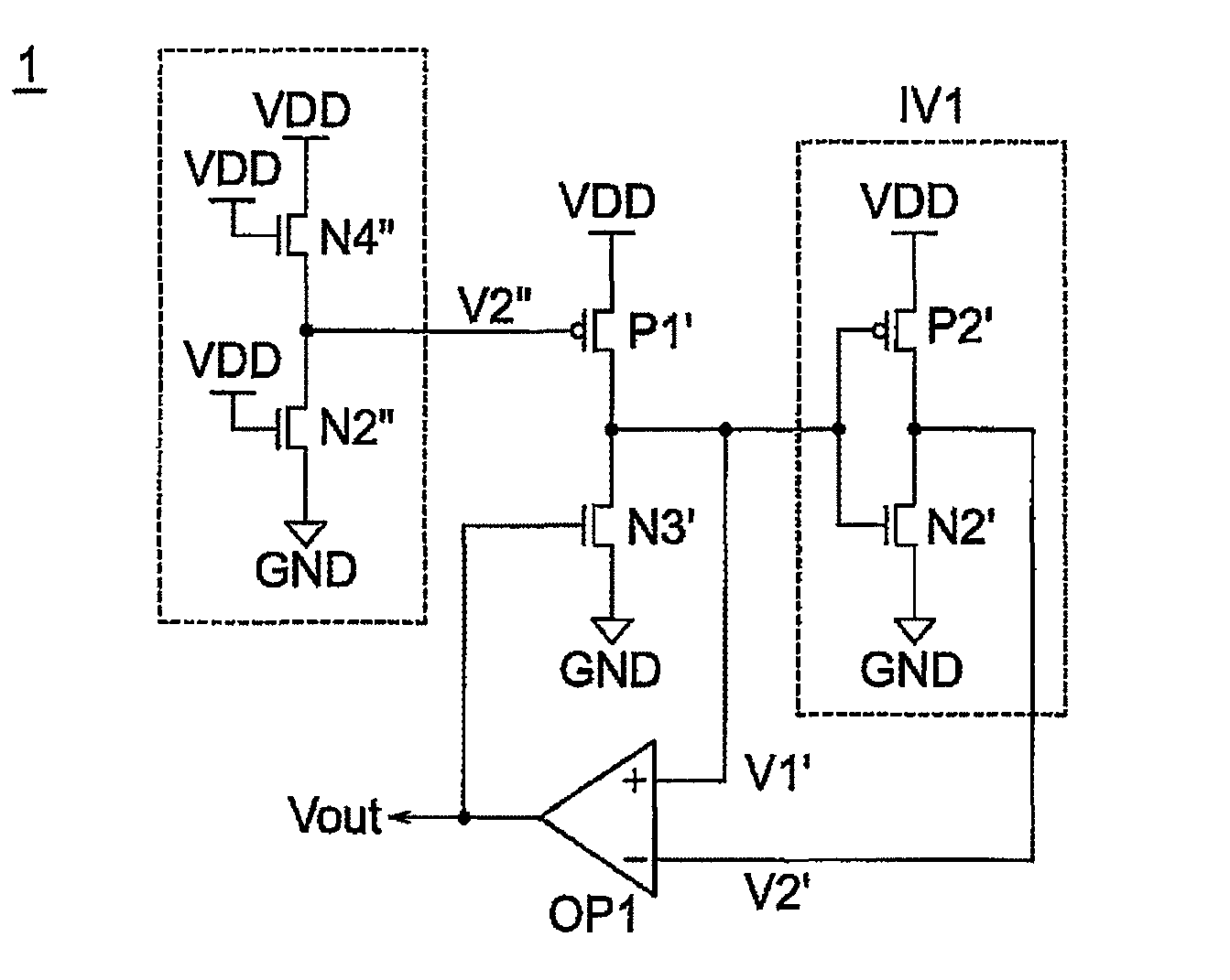
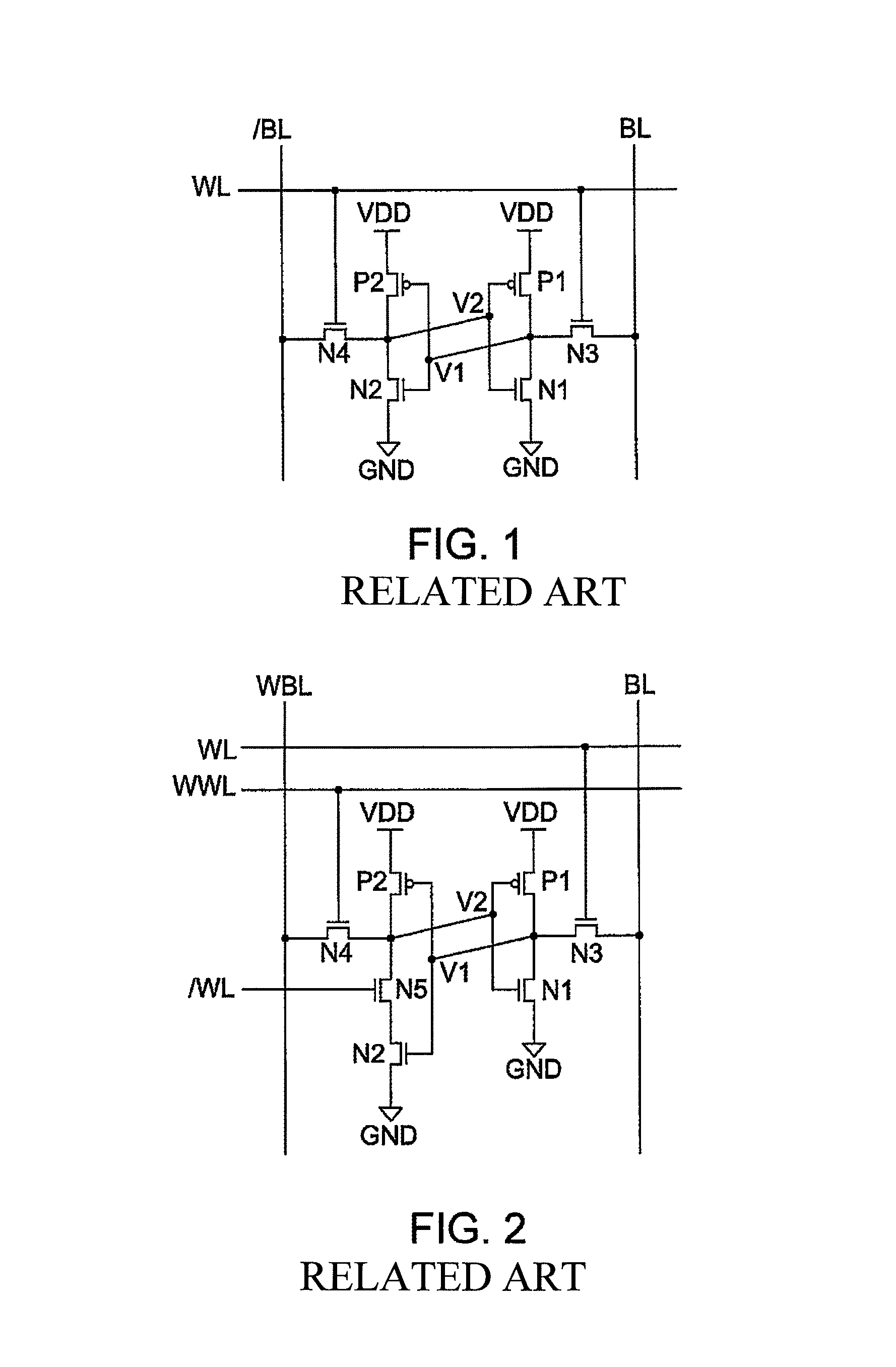
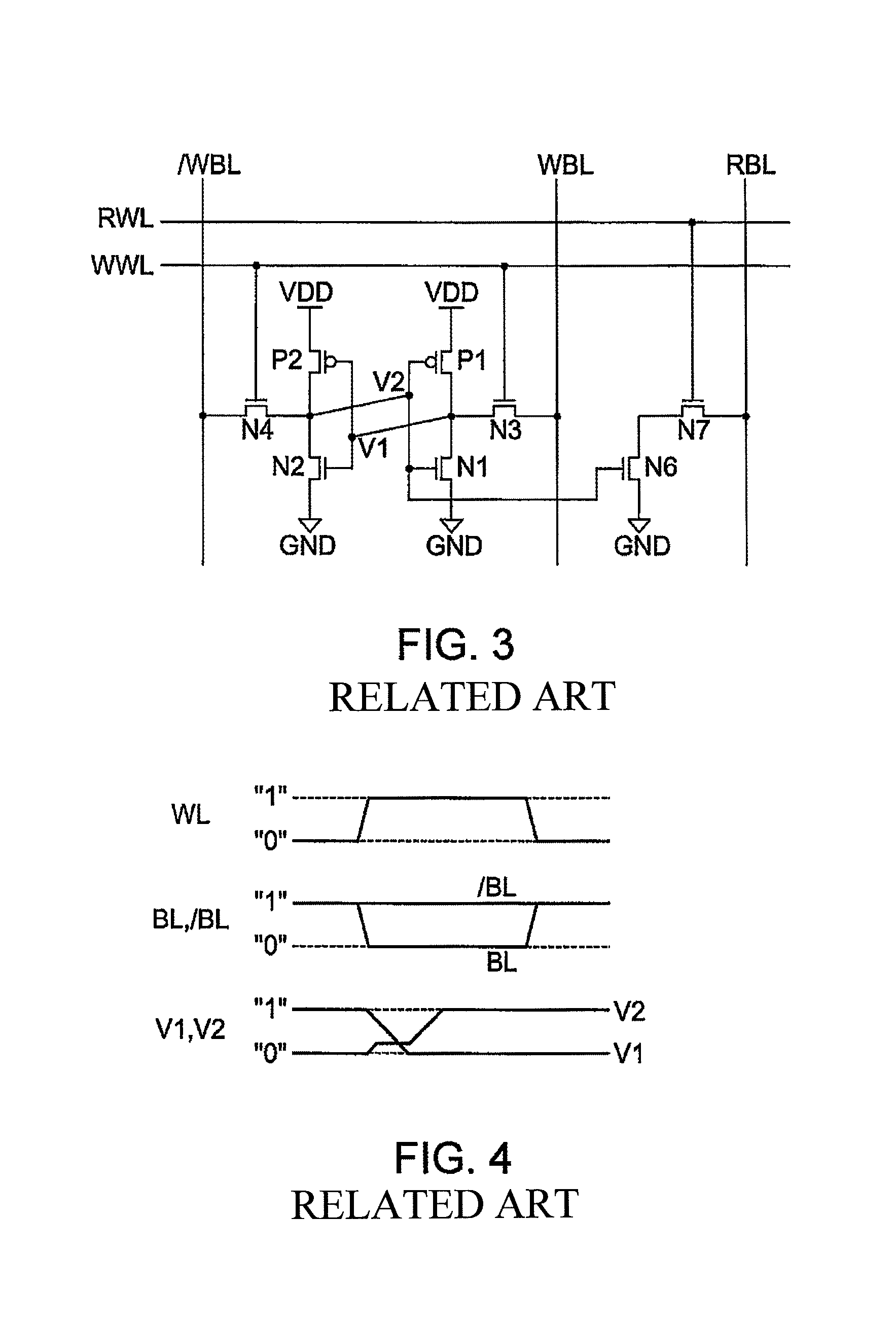
[0053]A writing margin monitoring circuit that monitors a margin at a writing operation will be described as Embodiment 1 of the present invention with reference to FIGS. 1 to 7. Known memory cell circuits respectively constructed from 6 transistors, 7 transistors and 8 transistors, to which a margin monitoring circuit and a method of controlling a power source of the present invention can be applied, are shown in FIGS. 1, 2 and 3. An operation waveform diagram for explaining a writing operation in the SRAM cell of FIG. 1 is shown in FIG. 4, and an explanatory drawing for explaining an essential condition to carry out a stable writing operation is shown in FIG. 5. A circuit diagram of a writing margin monitoring circuit diagram is shown in FIG. 6, and a circuit diagram of an operational amplifier configuring the writing margin monitoring circuit is shown in FIG. 7.

[0054]FIGS. 1, 2 and 3 are examples of a SRAM cell to which the present invention can be applied, and are diagrams respe...

embodiment 2

[0069]The case where the writing margin monitoring circuit of Embodiment 1 is used for control of a power source VDD_SRAM of a SRAM cell will be described as Embodiment 2 of the present invention with reference to FIGS. 8 to 12. FIG. 8 is a diagram showing a overall block in the case where the writing margin monitoring circuit 1 is used for control of the power source VDD_SRAM of the SRAM cell. A writing margin monitoring circuit 11 is shown in FIG. 9, a VDD2 voltage generator 12 that generates power source voltage VDD2 is shown in FIG. 10, and a connection diagram between a SRAM cell array 14 and a VDD selector 13 is shown in FIG. 11. Another writing margin monitoring circuit is shown as another embodiment in FIG. 12.

[0070]FIG. 8 is a diagram showing a block configuration in the case where the writing margin monitoring circuit is used for control of the power source VDD_SRAM of the SRAM cell. The present embodiment is an embodiment in which power source voltage VDD and second power...

embodiment 3

[0077]Embodiment 3 of the present invention will be described with reference to FIGS. 13 to 15. The present embodiment is an embodiment in which the writing margin monitoring circuit 11 and the VDD2 voltage generator 12 are integrated. FIG. 13 is a diagram showing a block configuration in the case where a writing margin monitor / voltage generator 31 is used for control of a high power source VDD_SRAM of a SRAM cell. A circuit diagram of a writing margin monitor / power source generator is shown in FIG. 14, and a circuit diagram of another writing margin monitor / power source generator is shown as another form in FIG. 15.

[0078]The writing margin monitor / voltage generator 31 shown in FIG. 14 integrates the writing margin monitoring circuit 11 of FIG. 9 and the voltage generator 12 of FIG. 10. In a writing margin monitoring circuit portion, a reference potential Vref is directly inputted as a gate input of a transistor N3′ that configures a simulation circuit. In a voltage generator portio...


PUM


Abstract

A voltage generator that monitors a writing margin as a control amount in order to carry out an optimum power source control when control of a SRAM cell power source is carried out at writing operation, and always keeps the writing margin constant; and a power source selector are included to switch power source voltage at writing. By switching the power source voltage at writing, a semiconductor memory device in which a stable writing operation is achieved without largely deteriorating writing time in the SRAM cell and an ultrahigh speed operation or ultralow power operation can be carried out is obtained.

Description

TECHNICAL FIELD[0001]The present invention relates to a semiconductor memory device, and particularly, the present invention relates to a semiconductor memory device that operates at ultrahigh speed and low voltage by controlling a power source of a SRAM cell so as to keep a writing margin constant, whereby a stable writing operation is achieved.BACKGROUND ART[0002]Semiconductor devices of recent years have become large-scaled and high speed, and a number of functions are incorporated and systematized. In these semiconductor devices, transistors are miniaturized for a large scale and high speed, whereby operation speed is improved. Further, for systematization, not only various functional blocks including a CPU but also various memory devices are mixed and mounted. In memory devices mixed and mounted on these system LSIs, for example, Static Random Access Memory (SRAM, hereinafter, referred to as a SRAM for short) mixed and mounted for use of a cache memory and the like, transistors...

Claims


Application Information

Patent Timeline
Patent Type & Authority Patents(United States)
IPC IPC(8): G11C7/00
CPCG11C5/147G11C11/417
Inventor TAKEDA, KOICHI
Owner NEC CORP
Why Eureka
Try Eureka