Semiconductor memory device and control method for semiconductor memory device

a semiconductor memory and memory device technology, applied in static storage, digital storage, instruments, etc., can solve the problems of reducing production yield, data readout error, and conventional semiconductor memory devices of the above-described type, and achieve the effect of increasing access time, occurrence probability, and increasing the probability of causing the defect of semiconductor memory devices

Inactive Publication Date: 2006-01-12
SOCIONEXT INC
View PDF7 Cites 6 Cited by
  • Summary
  • Abstract
  • Description
  • Claims
  • Application Information

AI Technical Summary

Benefits of technology

[0022] A problem occurs in that because of the transistor property fluctuation and the like, as the current drive capability of the replica memory cell transistor becomes higher than the current drive capability of the memory cell transistor, the data readout error proportionally increasingly occurs. In addition, a problem occurs in that as the current drive capability of the replica memory cell transistor becomes lower than the current drive capability of the memory cell transistor, the access time is proportionally increased. Further, a problem occurs in that as the number of the replica memory cells increases, the occurrence probability of the problems described above is increased, and the probability of causing semiconductor memory devices to be defective is increased.
[0023] As such, in the invention, the configuration is arranged such that at least one of replica memory cells are correlated with a plurality of memory cells, thereby reducing the number of replica memory cells [o1] required. This enables reducing, for example, the occurrence probability of increasing the access time and the occurrence probability of the data readout error, consequently enabling the problems described above to be prevented.

Problems solved by technology

However, conventional semiconductor memory devices of the above-described type have problems pending resolution.
However, since data required to be read out is “0”, a data readout error occurs.
This causes readout error and makes the semiconductor memory device to be a defective product, whereby to reduce the production yield.
However, in the event that the delay time (time from time T11a to T13a in the region R2 in FIG. 10) in the operation of the regular bit line BL is very long, the delay cannot be sufficiently corrected with the allowance time in accordance with timing correction.
This causes data readout error and makes the semiconductor memory device to be a defective product, whereby to reduce the production yield.

Method used


Image

  • Semiconductor memory device and control method for semiconductor memory device
  • Semiconductor memory device and control method for semiconductor memory device
  • Semiconductor memory device and control method for semiconductor memory device

Examples


first embodiment

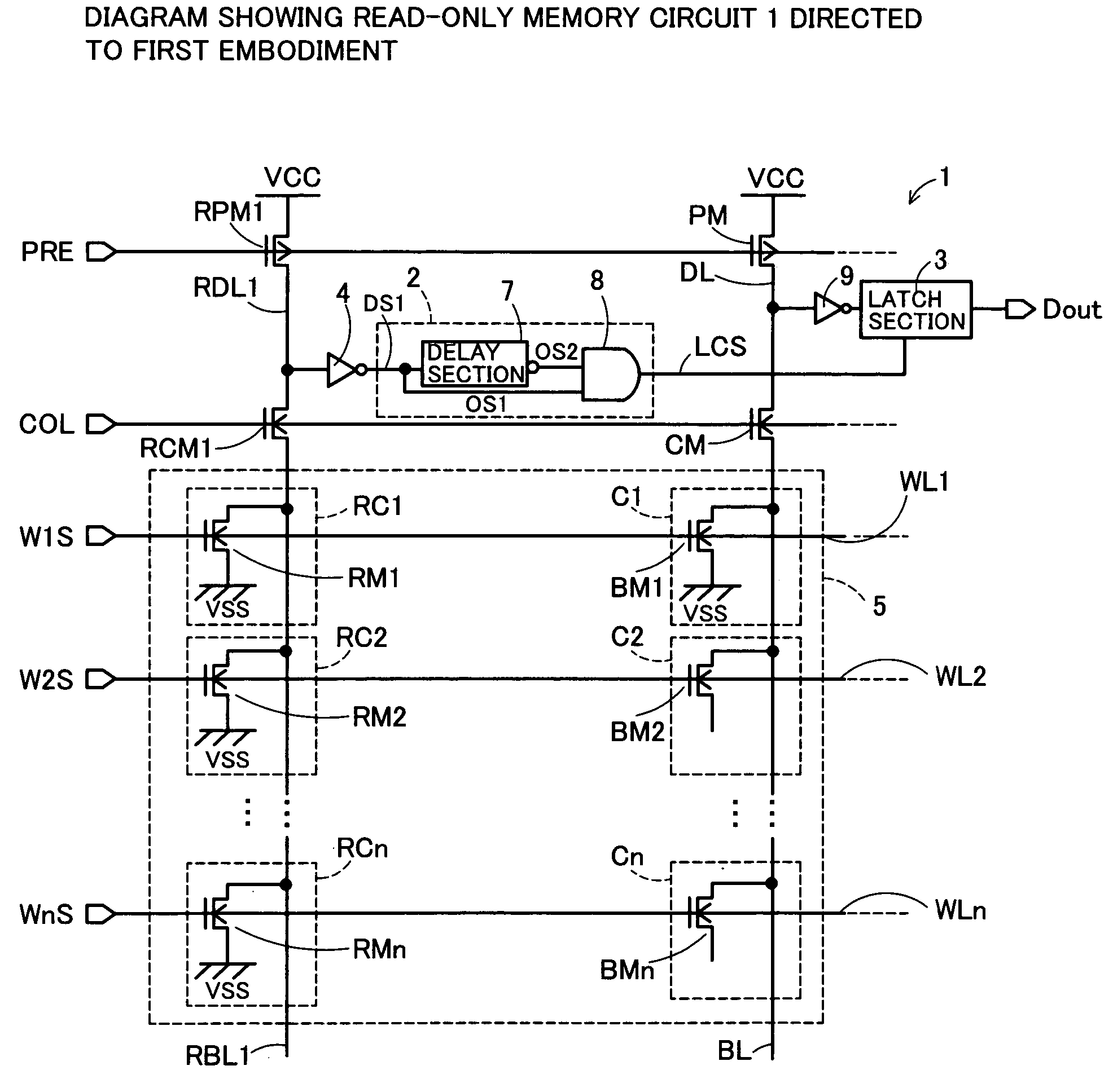
[0037] Practical embodiments related to semiconductor memory devices of the invention will be described herebelow with reference to FIGS. 1 to 7. To begin with, a first embodiment will be described with reference to FIGS. 1 to 3. Referring to FIG. 1, a ROM circuit 1 shown therein has a latch controller section 2, a latch section 3, and a cell section 5. Additionally, the ROM circuit 1 has a regular bit line BL and a regular data line DL; a first replica bit line RBL1 and a first replica data line RDL1; and first to n-th word lines WL1 to WLn (n=natural number). The regular bit line BL and the regular data line DL are interconnected through a transistor CM; and a first replica data line RDL1 and a first replica bit line RBL1 are interconnected through a transistor RCM1. The latch section 3 is connected to individual memory cells C1 to Cn through the regular data line DL and the regular bit line BL. The latch section 3 is controlled corresponding to a detection operation of the latch ...

second embodiment

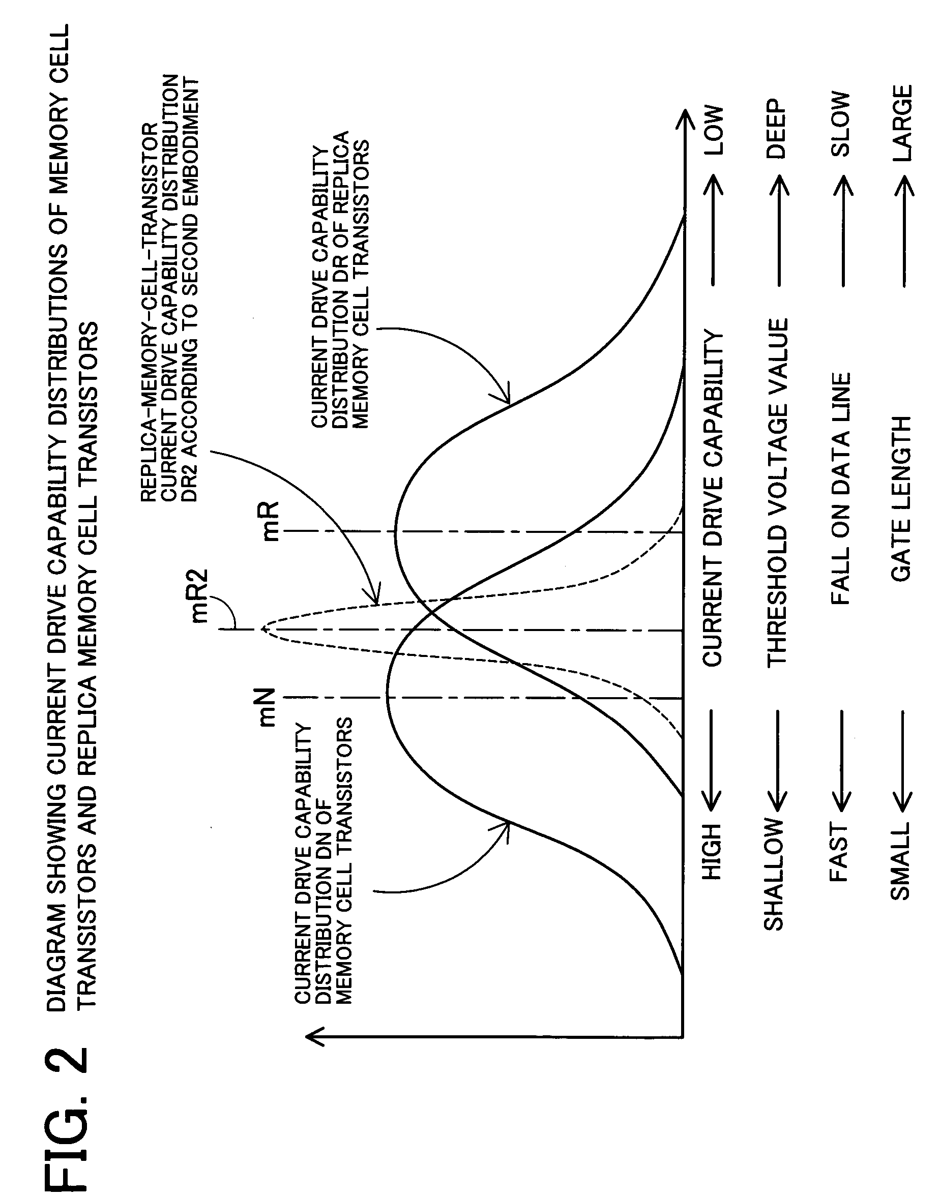
[0059] The following will describe effects and advantages of the embodiment. Replica memory cells fastest in readout operation are selected from the multiple replica memory cells connected to the multiple replica bit lines, whereby to enable obtaining the operation of narrowing the distribution itself in the current drive capabilities of the replica memory cell transistors (that is, transistor property fluctuation). More specifically, as represented by the replica-memory-cell-transistor current drive capability distribution DR2 shown in FIG. 2 of the second embodiment, the inter-replica-memory-cell-transistor current drive capability distribution (that is, transistor property fluctuation) can be narrowed and the distribution center can be shifted to an optimal position (i.e., shifted from the distribution center mR to the distribution center mR2) not causing problematic phenomena such as data readout error and access time increase. Thereby, the occurrence probability of the delay in...

third embodiment

[0079] The present invention is not limited to the embodiments, but various modifications and changes may of course be made without departing from the spirit and scope of the invention. While the third embodiment is arranged such that the production yield of semiconductor memory devices can be improved by performing the redundancy-and-recovery (or, redundancy relief) of the fixed replica memory cell, the embodiment is not limited thereto. The embodiment may be such that, for example, feedback control is performed to cause the current drive capability of a fixed replica memory cell transistor to conform to a predetermined value not causing the data readout error. A specific example of the above may be such that the value of current flowing into the fixed replica memory cell transistor is monitored, and value of a bias voltage to be applied to the gate of the fixed replica memory cell transistor is controlled corresponding to the current value so that the current value falls within a ...


PUM


Abstract

Provided is a semiconductor memory device using a single-bit line method that determines read operation timing in accordance with operation of a replica bit line. Further provided is a control method for the semiconductor memory device. Even when a transistor property fluctuation has occurred, the semiconductor memory device and the control method are capable of preventing, for example, increases in access time and circuit size and concurrently capable of reducing the occurrence probability of data readout error. The gate lengths of replica memory cell transistors are set as being values greater than the gate length of memory cell transistors. Thereby, a distribution center of a current drive capability distribution of the replica memory cell transistors is set lower than a distribution center of a current drive capability distribution of the memory cell transistors. Consequently, an occurrence probability of a delay in a voltage-fall start time on a regular data line can be reduced to be lower in comparison to a transmission timing of a latch control signal.

Description

CROSS-REFERENCE TO RELATED APPLICATIONS [0001] This application is based upon and claims the benefit of priority from each of the prior Japanese Patent Application No. 2004-204910 filed on Jul. 12, 2004, the entire contents of which are incorporated herein by reference. BACKGROUND OF THE INVENTION [0002] 1. Field of the Invention [0003] The invention relates to a semiconductor memory device in which data read timing is determined by operation of replica bit lines. The invention further relates to a control method for the semiconductor memory device. [0004] 2. Description of Related Art [0005]FIG. 8 shows a portion of a conventional read-only memory (“ROM”) circuit 100 using replica bit lines. The ROM circuit 100 has regular bit lines BL, regular data lines DL, replica bit lines RBL, and replica data lines RDL. Replica memory cells RC1 to RCn (n=natural number) are connected to each of the replica bit lines RBL, and memory cells C1 to Cn are connected to each of the regular bit lines...

Claims


Application Information

Patent Timeline
Patent Type & Authority Applications(United States)
IPC IPC(8): G11C7/06
CPCG11C7/06G11C2207/065G11C17/12G11C8/16
Inventor OZAWA, TAKASHI
Owner SOCIONEXT INC
Why Eureka
Try Eureka