Nonvolatile memory device, storage system having the same, and method of driving the nonvolatile memory device

a non-volatile memory and storage system technology, applied in the direction of information storage, static storage, digital storage, etc., can solve the problem of reducing the resistance of the pram

Active Publication Date: 2011-11-01
SAMSUNG ELECTRONICS CO LTD
View PDF26 Cites 41 Cited by
  • Summary
  • Abstract
  • Description
  • Claims
  • Application Information

AI Technical Summary

Benefits of technology

[0014]It is a separate feature of an embodiment to provide a nonvolatile memory device having improved reliability of a read operation.
[0016]It is a separate feature of an embodiment to provide a method of driving the nonvolatile memory device having improved reliability of a read operation.
[0027]The compensation current may compensate for a reduction in a level of the sensing node as a result of current flowing through a selected nonvolatile memory cell of the nonvolatile memory cell array.

Problems solved by technology

However, a resistance of the PRAM may decrease as temperature rises.
Further, in the case where the reset resistance greatly decreases, an operation error may occur in which the sense amplifier erroneously senses the reset state as the set state.

Method used


Image

  • Nonvolatile memory device, storage system having the same, and method of driving the nonvolatile memory device
  • Nonvolatile memory device, storage system having the same, and method of driving the nonvolatile memory device
  • Nonvolatile memory device, storage system having the same, and method of driving the nonvolatile memory device

Examples


Embodiment Construction

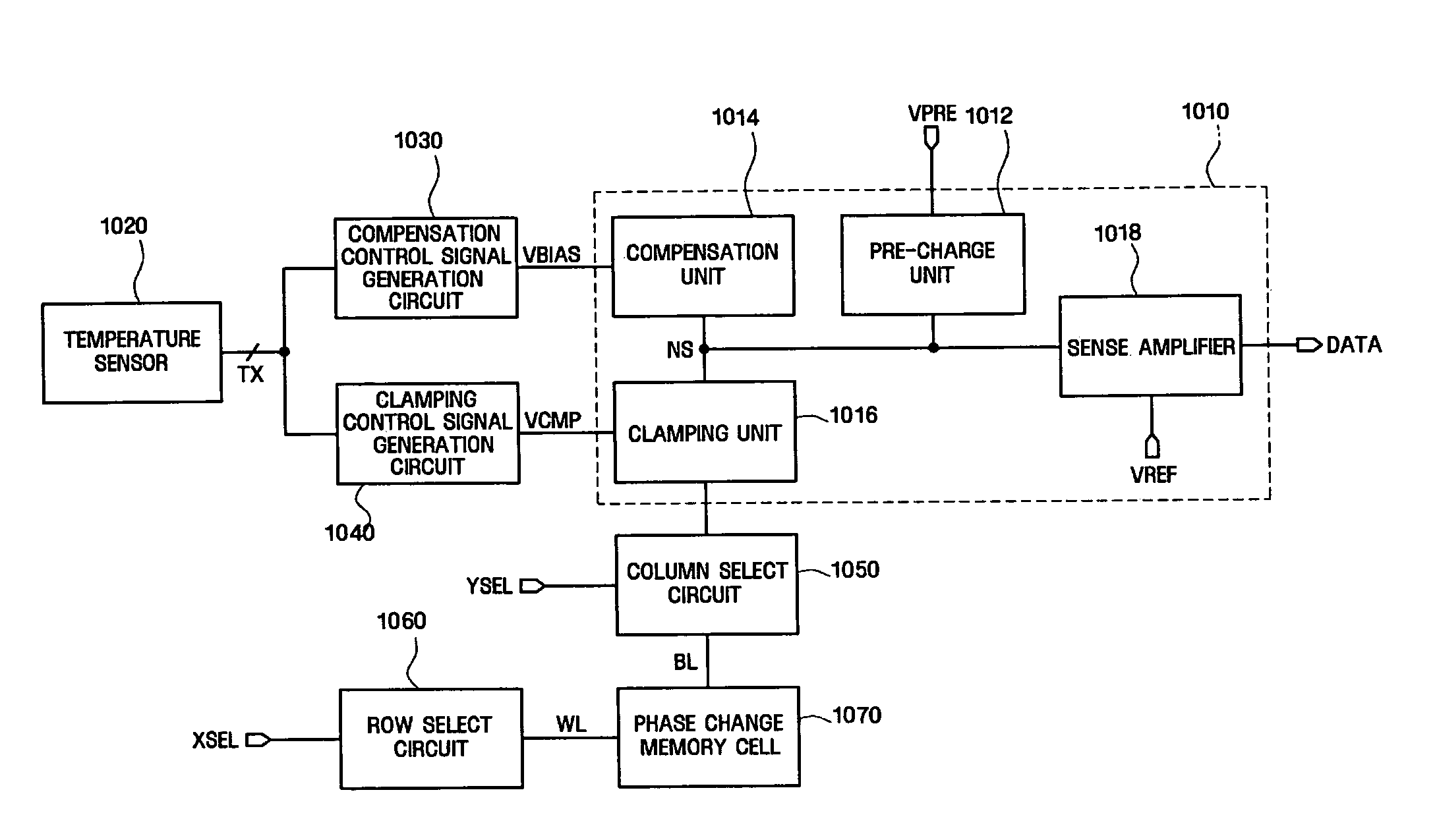
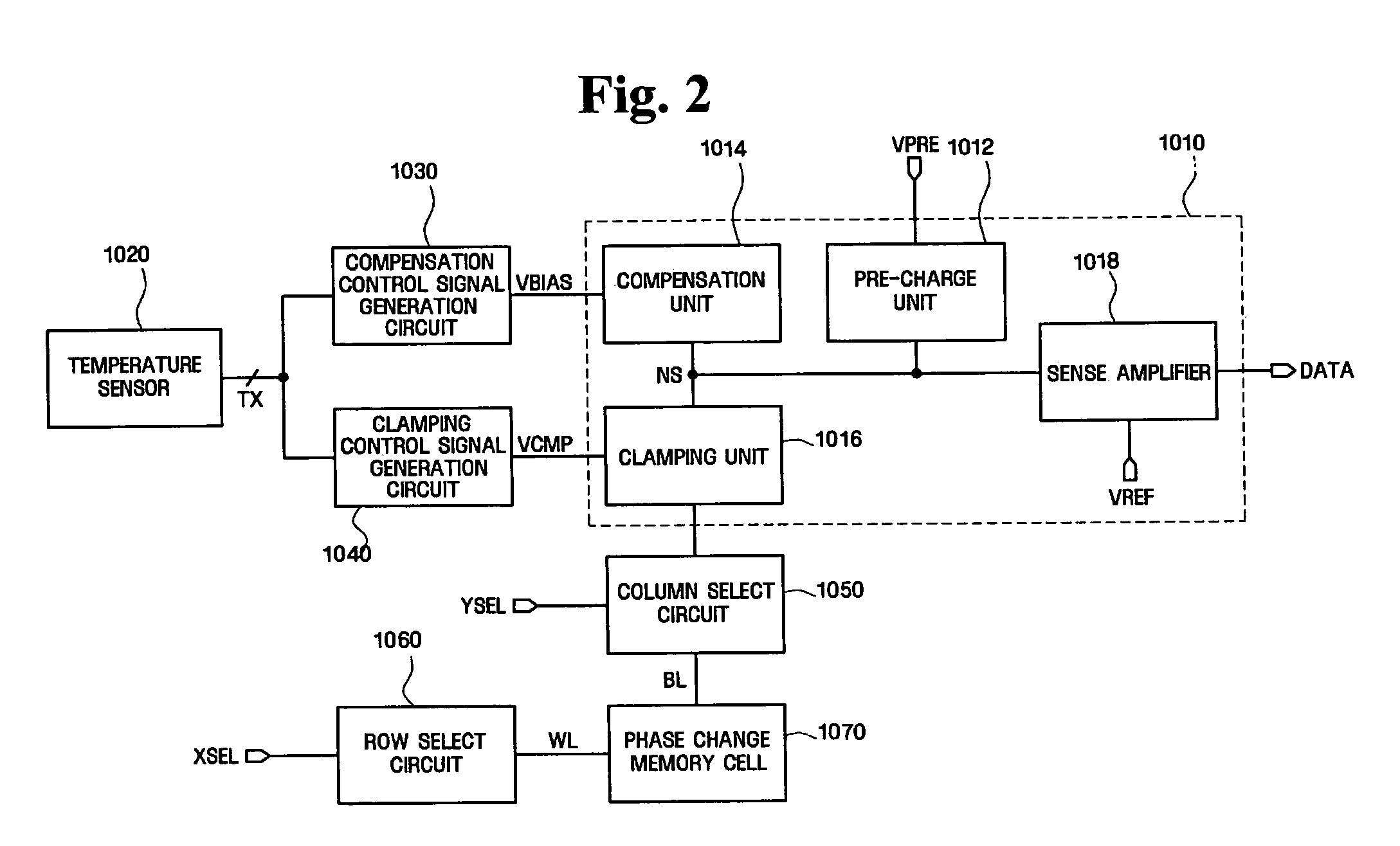
[0070]Korean Patent Application No. 10-2009-0101262, filed on Oct. 23, 2009, in the Korean Intellectual Property Office, and entitled: “Nonvolatile Memory Device, Storage System Having the Same, and Method of Driving the Nonvolatile Memory Device,” is incorporated by reference herein in its entirety. The contents of U.S. Pat. No. 7,245,605 (relating to write verify), U.S. Pat. No. 6,982,913 (relating to 2-step precharge), U.S. Pat. No. 7,215,592 (relating to global bitline), U.S. Pat. No. 7,315,469, and U.S. Patent Publication Nos. 2007 / 0236987 and 2008 / 0123389, which relate to nonvolatile memory devices, are incorporated by reference herein in their entireties.

[0071]Advantages and features and methods of accomplishing the same may be understood more readily by reference to the following detailed description of exemplary embodiments and the accompanying drawings. Features may, however, be embodied in many different forms and should not be construed as being limited to the embodiment...


PUM


Abstract

A nonvolatile memory device includes a memory cell array including a plurality of nonvolatile memory cells each having a resistance corresponding to one of a plurality of first resistance distributions, a temperature compensation circuit including one or more reference cells each having a resistance corresponding to one among one or more second resistance distributions, and a data read circuit including a compensation unit and a sense amplifier, the compensation unit being adapted to supply compensation current to a sensing node, an amount of the compensation current varying based on the resistance of each reference cell, and the sense amplifier being adapted to compare the level of the sensing node with a reference level and to output a comparison result.

Description

CROSS-REFERENCE TO RELATED APPLICATIONS[0001]This is a continuation-in-part application based on pending application Ser. No. 12 / 453,420 (now allowed), filed May 11, 2009, now U.S. Pat. No. 7,817,465 which is a continuation of application Ser. No. 11 / 896,721, filed Sep. 5, 2007, now U.S. Pat. No. 7,548,451, the entire contents of all of which are hereby incorporated by reference.BACKGROUND[0002]1. Field[0003]Embodiments relate to a nonvolatile memory device, a storage system having the same, and a method of driving the nonvolatile memory device, and more particularly, to a nonvolatile memory device having improved reliability of a read operation, a storage system including the nonvolatile memory device, and a method of driving the nonvolatile memory device.[0004]2. Description of the Related Art[0005]A phase Change Random Access Memory (PRAM) stores data using a phase change material, for example, a chalcogenide alloy. A state of the phase change material changes to a crystalline st...

Claims


Application Information

Patent Timeline
Patent Type & Authority Patents(United States)
IPC IPC(8): G11C11/00
CPCG11C7/04G11C8/12G11C11/5678G11C11/5685G11C13/0004G11C13/0007G11C13/004G11C2013/0054G11C2211/5634
Inventor BAE, JUN-SOOLEE, KWANG-JINCHO, BEAK-HYUNG
Owner SAMSUNG ELECTRONICS CO LTD
Why Eureka
Try Eureka