Method for prediction of premature dielectric breakdown in a semiconductor

a technology of premature dielectric breakdown and semiconductor, applied in the field of semiconductors, can solve the problems of inefficiency, high cost of tddb test, dielectric breakdown, etc., and achieve the effect of preserving the semiconductor wafer, predicting beol reliability efficiently and without destruction, and predicting beol reliability

Inactive Publication Date: 2011-11-08
GLOBALFOUNDRIES INC
View PDF19 Cites 4 Cited by
  • Summary
  • Abstract
  • Description
  • Claims
  • Application Information

AI Technical Summary

Benefits of technology

[0009]The invention predicts BEOL reliability efficiently and without destruction of the semiconductor wafer. Therefore, the invention predicts BEOL reliability quickly, while at the same time salvaging the semiconductor wafer. Further, the invention predicts BEOL reliability through the use of pre-existing comb-serpentine structures on the manufacturing line. Accordingly, the invention predicts BEOL reliability without costly modifications to existing manufacturing processes. Finally, the invention is implemented in real time. Accordingly, the invention reduces man hours and avails machines previously reserved for TDDB testing.
[0010]For at least the foregoing reasons, the invention improves upon premature dielectric breakdown prediction for semiconductors.

Problems solved by technology

Semiconductor defects cause dielectric breakdown.
Accordingly, TDDB test is expensive because of the associated dicing and packaging costs, e.g. operation of the ovens.
In addition, TDDB test is inefficient because the test period extends for over a month.
Finally, TDDB test wastes resources because both the wafer and the tested semiconductors are destroyed.
For at least these reasons, TDDB test is problematic.
IV test is inefficient to conduct on every chip because IV test requires the tedious study of IV plots such as shown in FIG. 2 for abrupt increases 205 or decreases 210 in leakage current.

Method used


Image

  • Method for prediction of premature dielectric breakdown in a semiconductor
  • Method for prediction of premature dielectric breakdown in a semiconductor
  • Method for prediction of premature dielectric breakdown in a semiconductor

Examples


Embodiment Construction

[0018]The invention will now be described with reference to the accompanying figures. In the figures, various aspects of the structures have been shown and schematically represented in a simplified manner to more clearly describe and illustrate the invention.

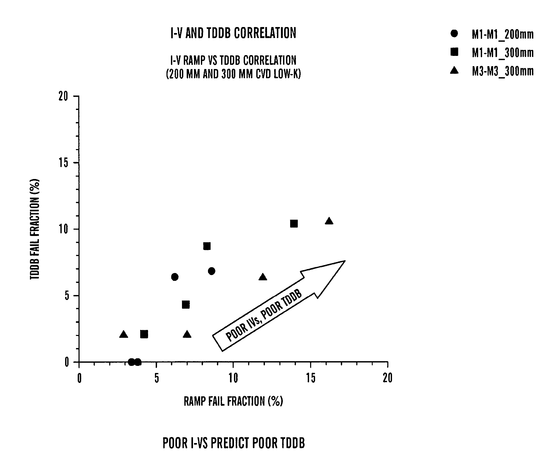
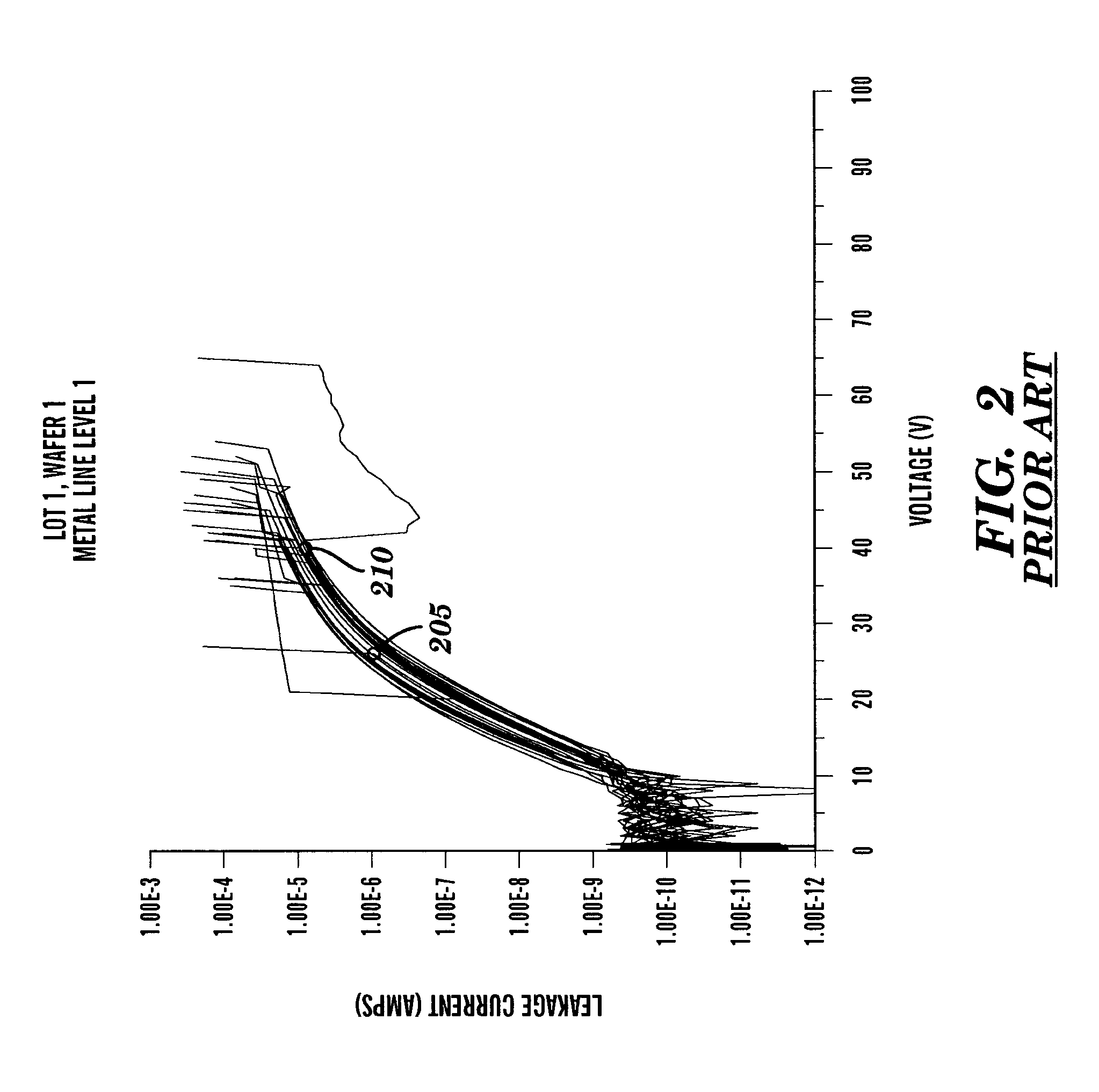
[0019]By way of overview and introduction, the invention comprises an improved method for efficiently predicting dielectric breakdown in the BEOL (“Back End of the Line”) that occurs in real time with minimal implementation cost and without destruction of the semiconductor wafer. The invention has application with respect to any dielectric material typically used to insulate interconnects in the BEOL, including but not limited to, SiO2, FTEOS, FSG, USG, SiCOH, p-SiCOH, as well as organic spin-on dielectrics such as SiLK, MSQ. Defects in semiconductors cause premature dielectric breakdown. Accordingly, by predicting premature dielectric breakdown in real time, the invention accomplishes an accurate assessment of the health of the...


PUM


Abstract

The invention predicts premature dielectric breakdown in a semiconductor. At least one dielectric breakdown mode is calculated for a layer within chips comprising a semiconductor wafer lot. If only one mode is calculated, that is the best calculated mode. If multiple modes can be calculated, a best mode that most accurately represents dielectric breakdown for the semiconductor wafer lot is determined. Premature dielectric breakdown will be associated with any semiconductor with a breakdown voltage less than a predetermined standard deviation from the best calculated mode.

Description

RELATED APPLICATIONS[0001]This application is a continuation in part application of co-pending U.S. patent application Ser. No. 11 / 160,213, entitled “METHOD FOR PREDICTION OF PREMATURE DIELECTRIC BREAKDOWN IN A SEMICONDUCTOR” filed on Jun. 14, 2005.BACKGROUND OF THE INVENTION[0002]1. Field of the Invention[0003]The invention relates generally to semiconductors and more particularly to predicting premature dielectric breakdown for semiconductors on a semiconductor wafer.[0004]2. Description of the Related Art[0005]Dielectric breakdown is important because dielectric breakdown provides an accurate measure of the Back End of the Line (“BEOL”) reliability of a semiconductor. Semiconductor defects cause dielectric breakdown. Therefore, when one monitors dielectric breakdown, one monitors the health of the manufacturing line.[0006]One prior art method for determining dielectric breakdown is time dependent dielectric breakdown (“TDDB”) test, which stresses a semiconductor at a constant vol...

Claims


Application Information

Patent Timeline
Patent Type & Authority Patents(United States)
IPC IPC(8): H01L21/00
CPCG06F17/5009G01R31/287G06F2217/10G06F2217/70G06F2217/78G06F30/20G06F2111/08G06F2117/02G06F2119/06
Inventor CHANDA, KAUSHIKRATHORE, HAZARA S.MCLAUGHLIN, PAUL S.EDWARDS, ROBERT D.CLEVENGER, LAWRENCE A.COWLEY, ANDREW P.YANG, CHIH-CHAOBARILE, CONRAD A.
Owner GLOBALFOUNDRIES INC
Why Eureka
Try Eureka