Self-organized pin-type nanostructures, and production thereof on silicon

a self-organized, silicon-based technology, applied in the direction of semiconductor/solid-state device manufacturing, basic electric elements, electric devices, etc., can solve the problems of high aspect ratio of nanostructures, high cost, and high cost, and achieve high aspect ratio and nano dimensions, the effect of avoiding or at least reducing the effort for dedicated masking

Active Publication Date: 2011-11-15
X FAB SEMICON FOUNDRIES
View PDF32 Cites 3 Cited by
  • Summary
  • Abstract
  • Description
  • Claims
  • Application Information

AI Technical Summary

Benefits of technology

[0010]It is an object of the invention to provide structures on silicon surfaces so as to have a high aspect ratio and nano dimensions, wherein an effort for a dedicated masking is to be avoided or at least to be reduced and wherein an enhanced behavior with respect to crystal faults and chemical surface contaminations is to be obtained compared to conventional techniques, wherein also a high degree of compatibility with further manufacturing processes should be obtained.

Problems solved by technology

These approaches are very flexible but are also complex and expensive.
For all mentioned techniques it is common that high aspect ratios of the nanostructures are not achieved, in particular when a low defect density is desired.
In the above cases, the nanostructure typically has an increased contamination density and / or an increased number of crystal faults after fabrication, when initially a single-crystalline silicon having a low crystal fault density was provided.
Therefore, these known techniques are usable in a restricted manner or with inferior results with respect to the overall performance of the device.
A significant disadvantage of this technique is the usage of metals in the plasma, which may result in an undesired contamination of the silicon.
The disadvantageous influences of even minute metal traces in the semiconductor manufacturing process, in particular for integrated circuits, are well known.
In addition to the contamination effect of the RIE tool due to addition of metals also the additional effort of these techniques in view of an application in manufacturing processes requiring high yield and reduced production cost is to be considered as a disadvantage.

Method used


Image

  • Self-organized pin-type nanostructures, and production thereof on silicon
  • Self-organized pin-type nanostructures, and production thereof on silicon
  • Self-organized pin-type nanostructures, and production thereof on silicon

Examples


Embodiment Construction

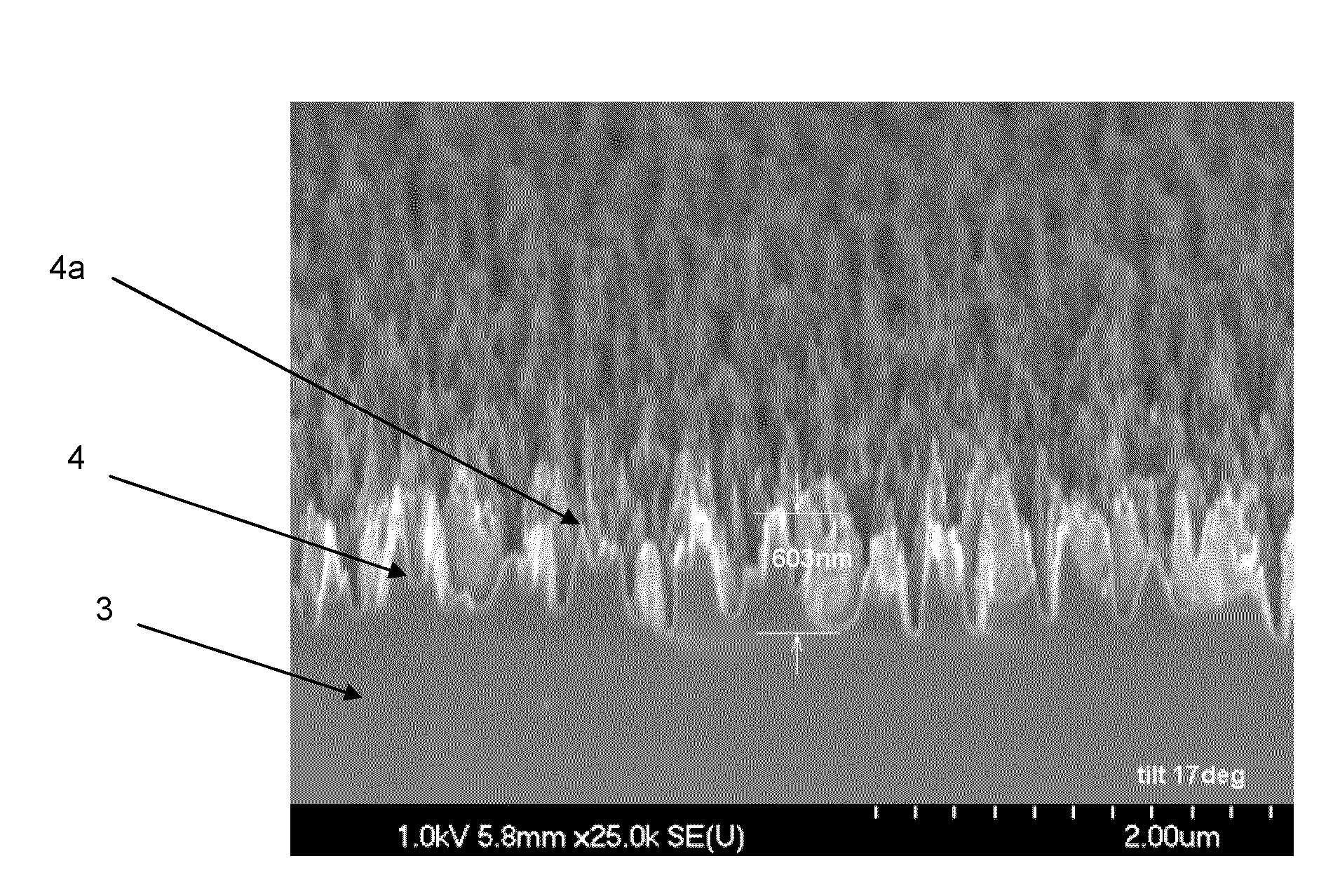
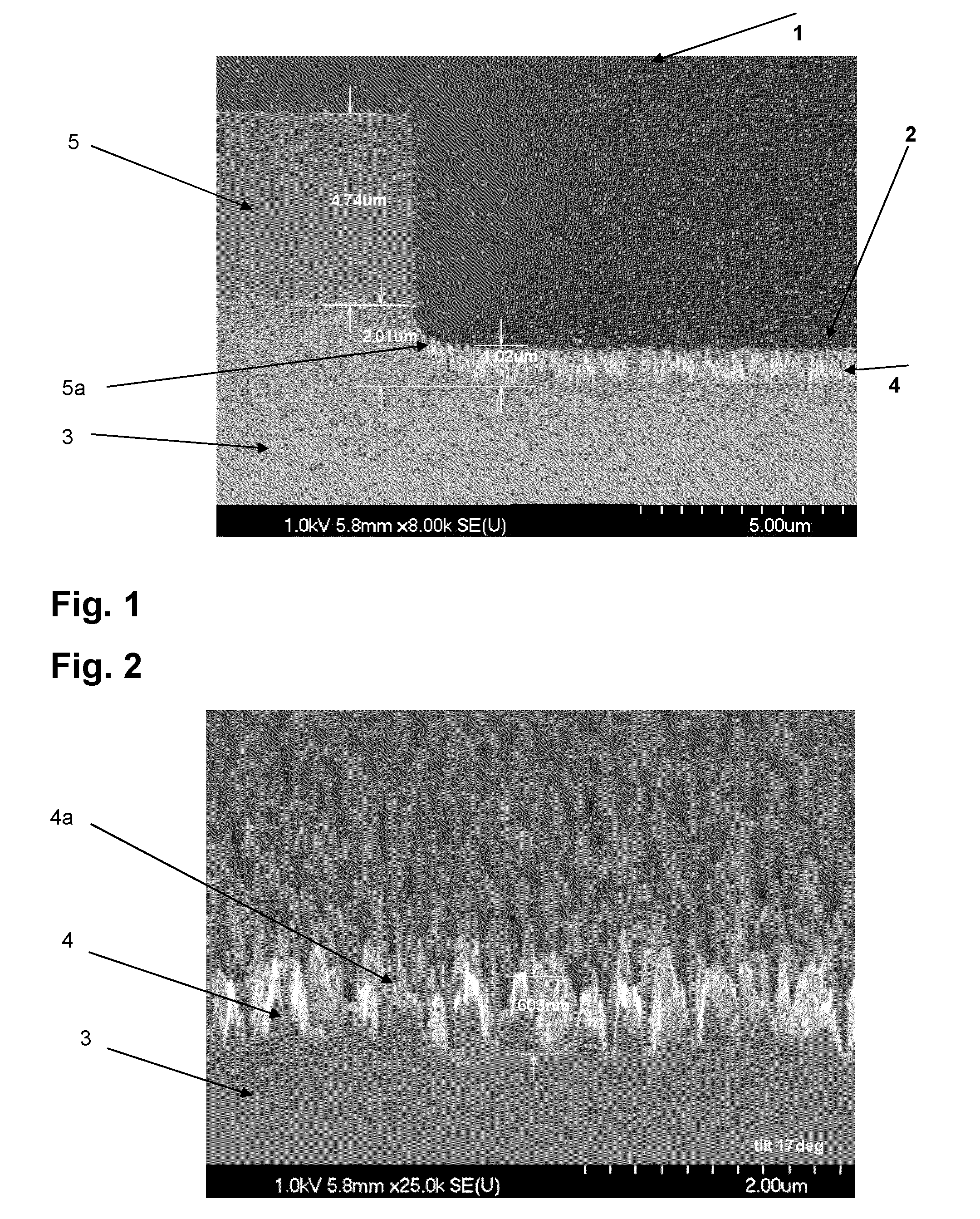
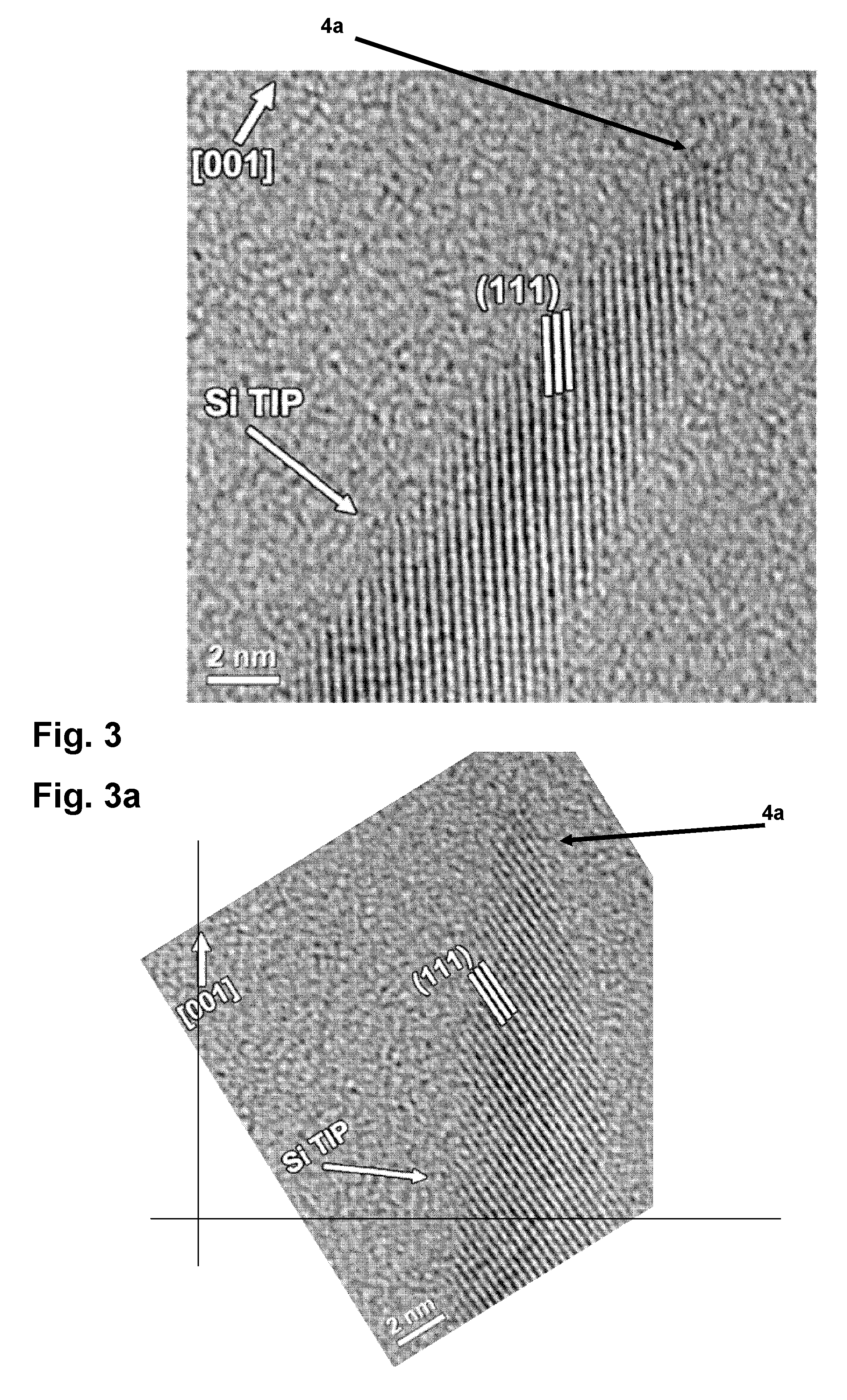
[0057]FIG. 1 illustrates a silicon-containing device 1 having a nanostructure 2 which comprises a single-crystalline silicon base layer 3 on which pin-type silicon structures 4 are formed. In this application pin-type silicon structures are to be understood as “pyramid-like” structures having a tip with lateral dimensions of a few nanometers, wherein the tip increases significantly in its lateral dimensions towards its bottom portion so that in a lower portion of the structure a lateral dimension of 10 nm or at least 100 nm is obtained. In this embodiment the silicon base layer 3 is delineated by a mask layer 5, which may be comprised of silicon dioxide, silicon nitride and the like, wherein the pin-type silicon structures 4 are formed up to an edge area 5a of the mask layer 5. In the embodiment shown the silicon base layer 3 is a part of a silicon wafer with a diameter of 6 inches and with a (100) surface orientation having a p-type doping that results in a specific resistivity of ...


PUM

PropertyMeasurementUnit
aspect ratioaaaaaaaaaa
pressureaaaaaaaaaa
temperatureaaaaaaaaaa

Abstract

By means of an RIE etch process for silicon (3), a pin-type structure (4,4a) without crystal defects is formed with high aspect ratio and with nano dimensions on the surface of silicon wafers without any additional patterning measures (e-beam, interference lithography, and the like) by selecting the gas components of the etch plasma in self-organization wherein, among others, a broadband antireflective behavior is obtained that may be applicable in many fields.

Description

FIELD OF THE INVENTION[0001]The invention generally relates to the fabrication of patterned or structured silicon surfaces and in particular relates to the creation of pin-type structures having nano dimensions in the range below, for instance, the wavelength of visible light, wherein hereinafter these structures are referred to as nanostructures.RELATED ART[0002]Many electronic, opto-electronic, sensoric and micromechanical devices comprise silicon as a component in doped and / or undoped, crystalline and / or polycrystalline and / or amorphous state. In order to meet the corresponding device specific requirements the silicon has therefore usually to be processed accordingly, which frequently involves a patterning of the silicon.[0003]For the patterning of silicon usually a mask of photoresist is generated, by means of which the removal is controlled by an etch process, for example WO-A 2005 / 045941. In order to generate small structures or patterns by means of a resist mask the photoresi...

Claims


Application Information

Patent Timeline
Patent Type & Authority Patents(United States)
IPC IPC(8): H01L21/00
CPCH01L21/3065H01L21/3086H01L21/32137H01L21/32139
Inventor BACH, KONRADGAEBLER, DANIELFISCHER, MICHAELSTUBENRAUCH, MIKE
Owner X FAB SEMICON FOUNDRIES
Why Eureka
Try Eureka