Semiconductor package with stacked dice for a buck converter

a technology of buck converter and stacked dice, which is applied in the direction of semiconductor devices, semiconductor/solid-state device details, electrical equipment, etc., can solve the problems of large parasitic capacitance and inductance, and the prior art buck converter requires a relatively large footprint, so as to reduce the footprint of the device, and dissipate heat

Active Publication Date: 2011-11-22
SEMICON COMPONENTS IND LLC
View PDF12 Cites 1 Cited by
  • Summary
  • Abstract
  • Description
  • Claims
  • Application Information

AI Technical Summary

Benefits of technology

[0005]An advantage of the present invention is the large surface area of the high side drain that is available to conduct heat. Such a stacked dice configuration both reduces the footprint of the device and helps to dissipate any heat that may be produced by the package during operation. Another advantage of the present invention is that it can reduce the parasitic capacitances and inductances due to both low side die (drain) and high side die (source) sharing the same die attach pad. The reduction of the parasitic capacitances and inductances also reduces the switching losses of the buck converter, and enables the use of higher switching frequencies. Such a reduction further reduces losses and improves power-conversion efficiency.
is the large surface area of the high side drain that is available to conduct heat. Such a stacked dice configuration both reduces the footprint of the device and helps to dissipate any heat that may be produced by the package during operation. Another advantage of the present invention is that it can reduce the parasitic capacitances and inductances due to both low side die (drain) and high side die (source) sharing the same die attach pad. The reduction of the parasitic capacitances and inductances also reduces the switching losses of the buck converter, and enables the use of higher switching frequencies. Such a reduction further reduces losses and improves power-conversion efficiency.

Problems solved by technology

Unfortunately, prior art buck converters require a relatively large footprint.
Additionally, prior art buck converters require extensive wirebonding and involve complex electrical paths which result in larger parasitic capacitances and inductances.

Method used


Image

  • Semiconductor package with stacked dice for a buck converter
  • Semiconductor package with stacked dice for a buck converter
  • Semiconductor package with stacked dice for a buck converter

Examples


Embodiment Construction

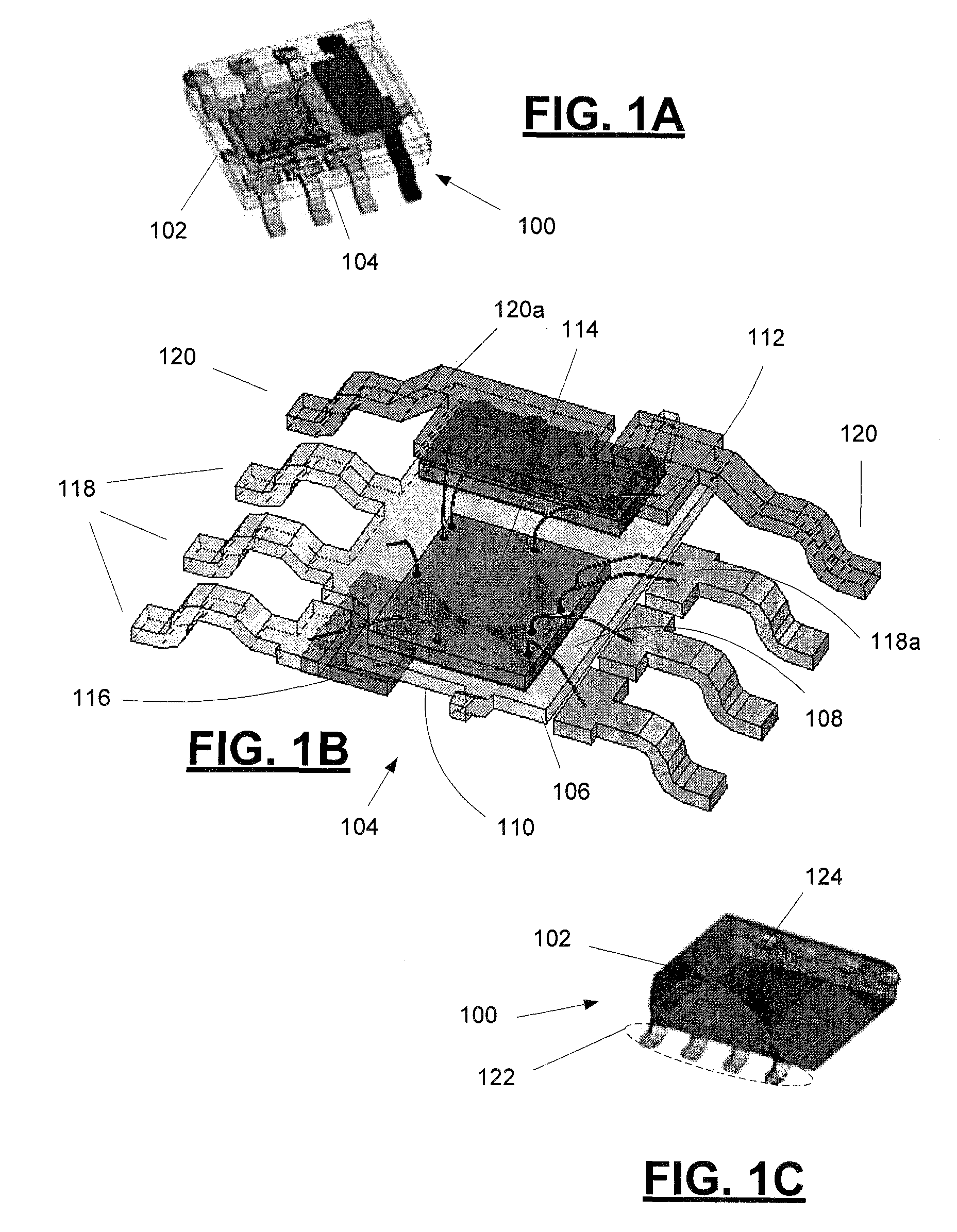
[0017]Referring to FIG. 1A, buck converter package 100 is shown enclosed in molding compound 102. For the sake of illustration, molding compound 102 has been shown in phantom. The assembly 104 is disposed within molding compound 102 and is shown in more detail in FIG. 1B.

[0018]Referring now to FIG. 1B, assembly 104 is comprised of conductive die attach pad 106, which has a first surface 108 and a second surface 110, opposite first surface 108. Low side die 112 and controller die 114 are mounted on first surface 108. High side die 116 is mounted on second surface 110 of die attach pad 106. As will be described in detail elsewhere in this application, low side die 112 is a flip chip die with its drain placed in electrical communication with the source of high side die 116 through conductive die attach pad 106. High side die 116 is also a flip chip die. Electrical connections are made between the components of the assembly 104 and the environment outside of the molding compound 102 (se...


PUM


Abstract

Disclosed in this specification is a buck converter package with stacked dice and a process for forming a buck converter. The package includes a die attach pad with a low side die mounted on one surface and a high side die mounted on the opposing surface. The die attach pad is conductive, such that the drain of the low side die is connected to the source of the high side die through the pad. A controller die controls the gates of the high and low side dies. A plurality of leads extends outside of the package to permit electrical connections to the inside of the package. The high side drain is exposed to one of the surfaces of the package.

Description

FIELD OF THE INVENTION[0001]This invention relates, in one embodiment, to a flip leaded molded package (FLMP) with stacked dice for a buck converter and a process for forming the same. The buck converter is encased within a molding compound such that leads extend from the internal components to the outside of the package. The drain of the high side die is exposed to an external surface of the package. The source of the high side drain is electrically connected to the drain of the low side die through a conductive die attach pad.BACKGROUND OF THE INVENTION[0002]Buck converters are conventionally used to convert an input voltage to a lower, output voltage. A synchronous buck converter uses a high side die (which is coupled to the input voltage) and a low side die (which is coupled to ground) connected in series. The operation of the high side and low side dies is controlled by a controller die. The controller die operates the high side and low side gates to produce the desired duty cy...

Claims


Application Information

Patent Timeline
Patent Type & Authority Patents(United States)
IPC IPC(8): H01L23/495
CPCH01L24/40H01L24/97H01L23/49562H01L23/49575H01L2224/48091H01L2924/181H01L2924/07802H01L2224/40247H01L2224/48137H01L2924/01033H01L24/49H01L24/48H01L2224/48247H01L2224/49171H01L2924/01027H01L2924/01029H01L2924/01046H01L2924/01082H01L2924/30107H01L23/3107H01L2924/00014H01L2924/00H01L2924/00012H01L24/41H01L2224/4103H01L2224/16245H01L2224/49113H01L24/84H01L24/38H01L2224/841H01L2224/8385H01L2224/32245H01L2224/38H01L2224/45099H01L2224/45015H01L2924/207H01L2224/37099H01L2224/84H01L2224/73221
Inventor LIU, YONGNEWBERRY, WILLIAMRIOS, MARGIE T.QIAN, QIUXIAO
Owner SEMICON COMPONENTS IND LLC
Why Eureka
Try Eureka