
Field electron emission source having carbon nanotubes and method for manufacturing the same

a field electron emission source and carbon nanotube technology, which is applied in the manufacture of electric discharge tubes/lamps, discharge tube main electrodes, and electrode systems, etc., can solve the problems of low field electron emission efficiency of field electron emission sources and inability to accurately control the formation of electron emission portions

Active Publication Date: 2011-12-06
TSINGHUA UNIV +1
View PDF6 Cites 2 Cited by
  • Summary
  • Abstract
  • Description
  • Claims
  • Application Information

AI Technical Summary

Benefits of technology

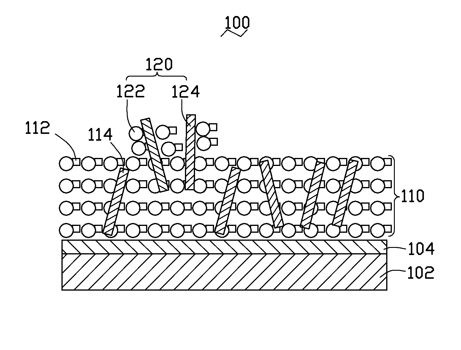
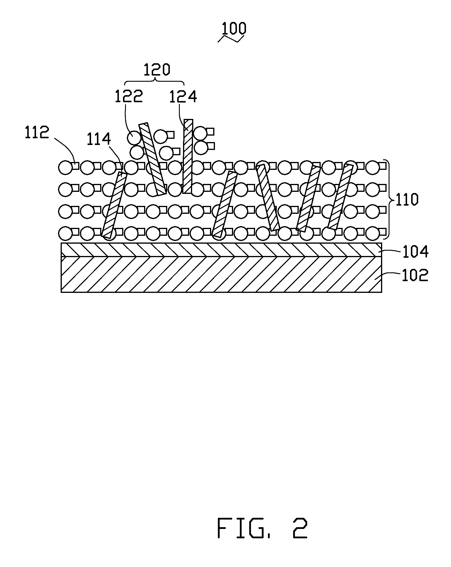
[0009]The present method for manufacturing the field electron emission source can have the following advantages over conventional methods. First, the method can be performed rapidly and easily due to a high energy density of the laser beam. Secondly, the field electron emission source has a high resolution because the laser beam creates a sharp edge on the electron emission portion. Thirdly, the electron emission portions of the field electron emission source can be accurately selected by controlling the movement of the laser beam. Lastly, the field electron emission source has high field emission efficiency due to protruding CNTs in the electron emission portion.

Problems solved by technology

However, in this mechanical method, the formation of the electron emission portions cannot be accurately controlled.
Further, the field electron emission source has a low field electron emission efficiency due to a shielding effect caused by closer, adjacent CNTs.

Method used


Image

  • Field electron emission source having carbon nanotubes and method for manufacturing the same
  • Field electron emission source having carbon nanotubes and method for manufacturing the same
  • Field electron emission source having carbon nanotubes and method for manufacturing the same

Examples


Embodiment Construction

[0017]Reference will now be made to the drawings to describe preferred and exemplary embodiments of the present invention in detail.

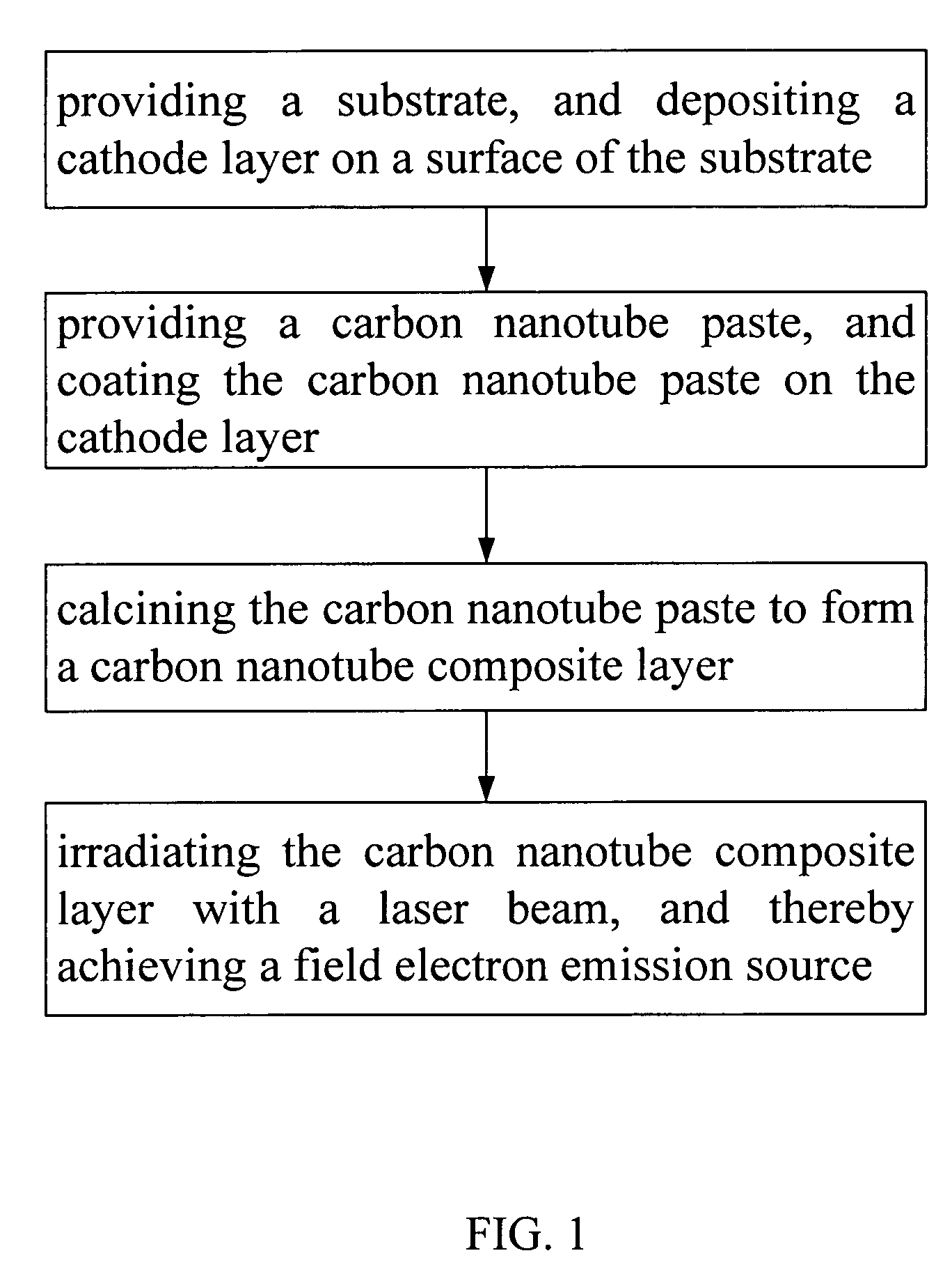
[0018]Referring to FIG. 1, a method for manufacturing a field electron emission source includes the steps of:

(a) providing a substrate, and depositing a cathode layer on a surface of the substrate;

(b) providing a carbon nanotube (CNT) paste and coating the CNT paste on the cathode layer;

(c) calcining the CNT paste to form a CNT composite layer; and

(d) irradiating the CNT composite layer with a laser beam of a certain power density, thereby achieving a field electron emission source.

[0019]In step (a), a pattern of the cathode layer is deposited in a predetermined region on a surface of the substrate by a conventional method, such as the sputtering method. The substrate can be made of any suitable material, e.g., glass, plastic, or metal. The cathode layer is made of one or more conductive metal materials, e.g., gold, silver, copper, or any one of their a...


PUM

PropertyMeasurementUnit
lengthaaaaaaaaaa
diametersaaaaaaaaaa
electric fieldaaaaaaaaaa

Abstract

An exemplary method for manufacturing a field electron emission source includes: providing a substrate (102); depositing a cathode layer (104) on a surface of the substrate; providing a carbon nanotube paste, coating the carbon nanotube paste on the cathode layer; calcining the carbon nanotube paste to form a carbon nanotube composite layer (110); and, irradiating the carbon nanotube composite layer with a laser beam of a certain power density, thereby achieving a field electron emission source.

Description

BACKGROUND[0001]1. Field of the Invention[0002]The present invention relates to field electron emission sources having carbon nanotubes and methods for manufacturing the same.[0003]2. Discussion of Related Art[0004]Field emission displays (FEDs) are a relatively new and rapidly developing flat panel display technology. Compared to conventional technologies, e.g., cathode-ray tube (CRT) and liquid crystal display (LCD) technologies, field emission displays are superior in having a wider viewing angle, lower energy consumption, a smaller size, and a higher quality display. A field electron emission source is an essential component in FEDs and has been widely investigated in recent years.[0005]Carbon nanotubes (CNTs) are very small tube-shaped structures, essentially having a composition of a graphite sheet rolled into a tube. CNTs produced by arc discharge between graphite rods were discovered and reported in an article by Sumio Iijima entitled “Helical Microtubules of Graphitic Carbo...

Claims


Application Information

Patent Timeline
Patent Type & Authority Patents(United States)
IPC IPC(8): H01J9/02H01J9/00
CPCH01J9/025H01J29/04H01J31/127H01J2201/30469
Inventor CHEN, ZHUOZHU, FENGJIANG, KAI-LILIU, LIANGFAN, SHOU-SHAN
Owner TSINGHUA UNIV
Learn More