Metrology and 3D reconstruction of devices in a wafer

a technology of 3d reconstruction and devices, applied in the field of metalrology, can solve the problems of cp giving inaccurate results, generating incorrect measurements, and foregoing snv methods

Inactive Publication Date: 2012-01-17
WESTERN DIGITAL TECH INC
View PDF12 Cites 152 Cited by
  • Summary
  • Abstract
  • Description
  • Claims
  • Application Information

AI Technical Summary

Benefits of technology

[0006]Various embodiments of the present invention solve the foregoing problem by providing metrology and 3D reconstruction methods for measuring three-dimensional devices in a wafer. Rather than only making successive cuts in a single device, successive cuts are made in nearby devices on the wafer. Because these nearby devices are designed to be geometrically identical (e.g., a wafer may contain thousands of write poles of a single design), a composite 3D reconstruction utilizing cross-sectional measurements of separate devices can provide information about the geometry of all the devices.

Problems solved by technology

Unfortunately, the foregoing SnV method can generate incorrect measurements in small devices in a wafer, such as PMR write poles, as each succeeding CP measurement may be distorted by the preceding cuts (e.g., the measurement of the CP may give inaccurate results as the relative distance between the fiducial and the new cut may have been changed by the intervening cuts).

Method used


Image

  • Metrology and 3D reconstruction of devices in a wafer
  • Metrology and 3D reconstruction of devices in a wafer
  • Metrology and 3D reconstruction of devices in a wafer

Examples


Embodiment Construction

[0019]In the following detailed description, numerous specific details are set forth to provide a full understanding of the present invention. It will be apparent, however, to one ordinarily skilled in the art that the present invention may be practiced without some of these specific details. In other instances, well-known structures and techniques have not been shown in detail to avoid unnecessarily obscuring the present invention.

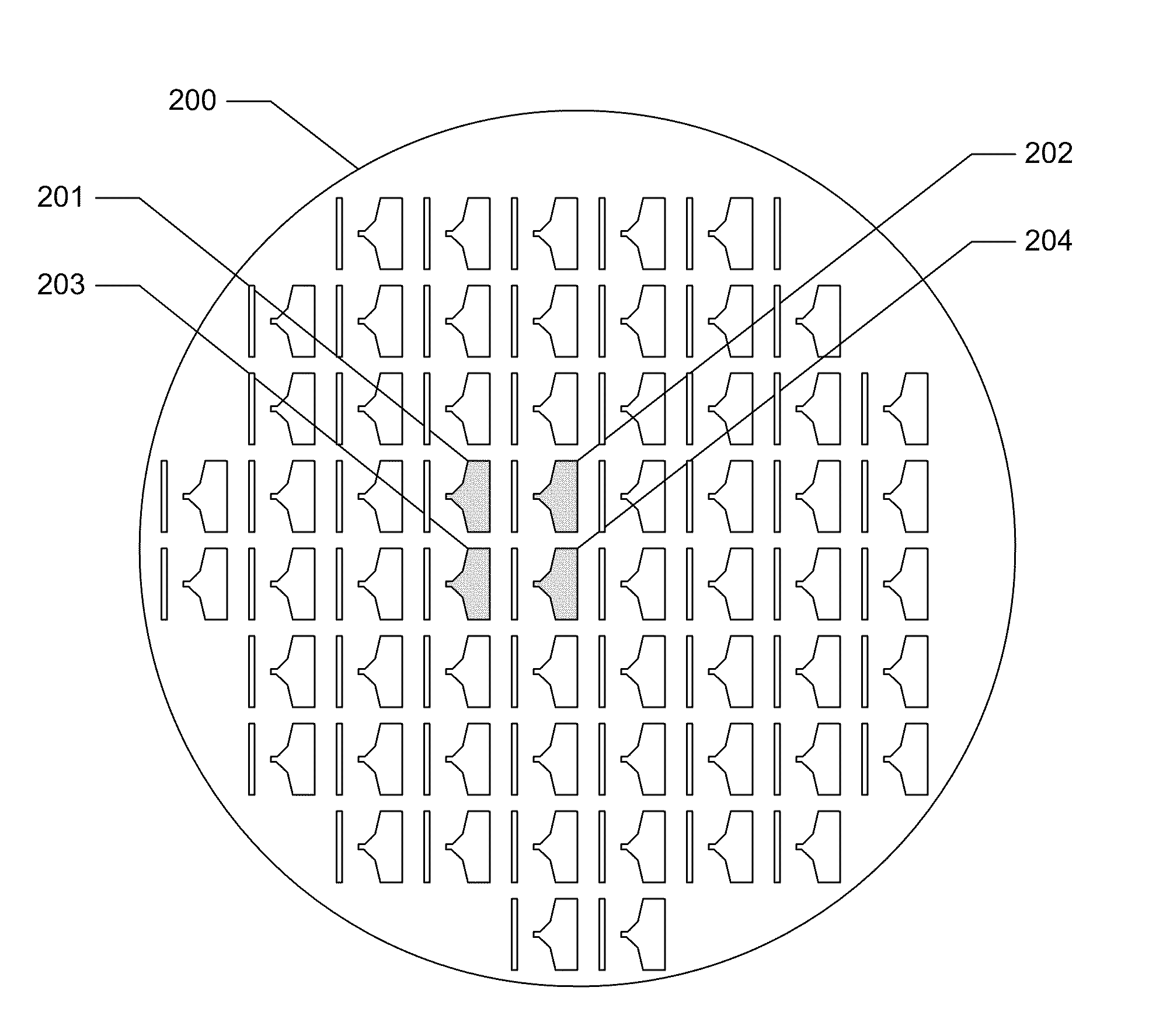
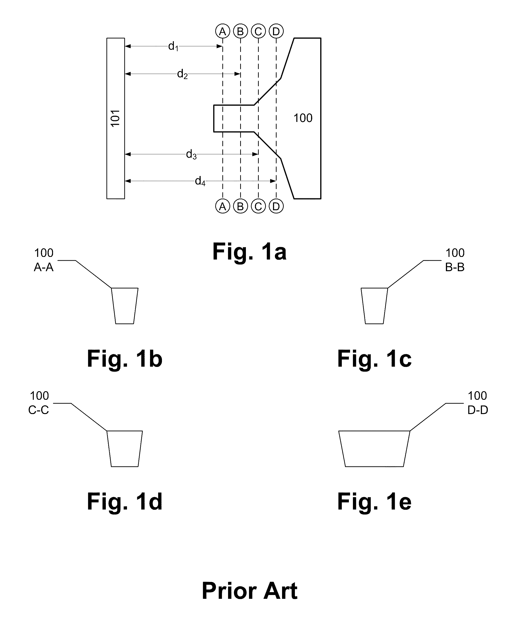
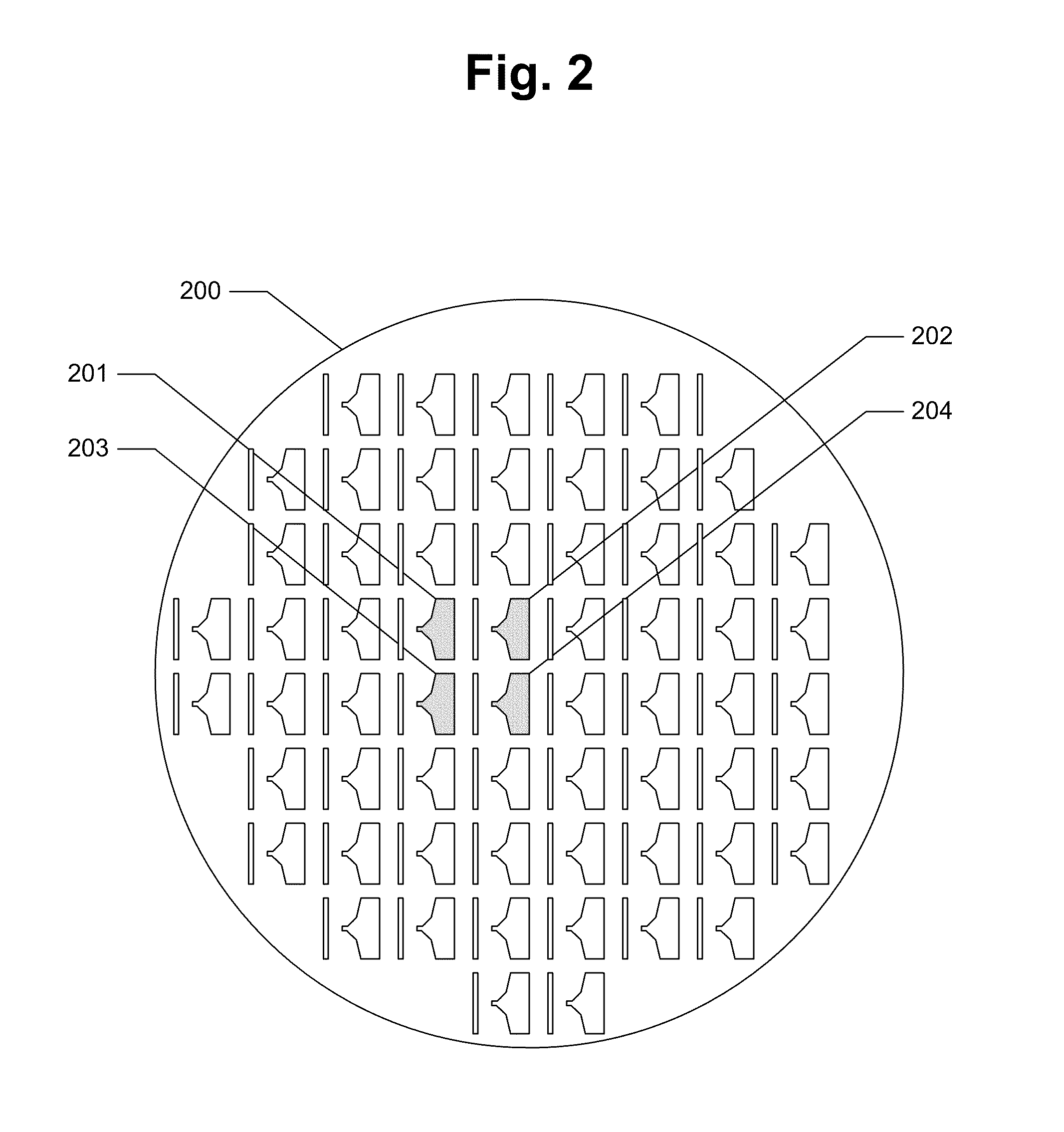
[0020]FIG. 2 illustrates an exemplary wafer layout in which a plurality of 3D devices are disposed, in accordance with one aspect of the subject disclosure. Wafer 200 includes a plurality of devices with substantially identical geometries (e.g., devices with the same design parameters, and which are different from one another to the extent that process variations dictate). To determine the geometry of the devices, cross-sectional images from several nearby devices, such as devices 201-204, can be taken and reconstructed to provide composite information ab...


PUM

PropertyMeasurementUnit
distanceaaaaaaaaaa
scanning electron microscopyaaaaaaaaaa
distancesaaaaaaaaaa

Abstract

A method for measuring three-dimensional devices in a wafer comprises the step of obtaining a plurality of cross-sectional images of a corresponding plurality of three-dimensional devices in the wafer. The plurality of three-dimensional devices have essentially identical geometries. Each cross-sectional image is obtained from a plane in the corresponding three-dimensional device at a predetermined distance from a fiducial mark thereof. The predetermined distance is different for each of the plurality of cross-sectional images. The method further comprises the step of determining the geometries of the plurality of three-dimensional devices based on the cross-sectional images thereof.

Description

FIELD OF THE INVENTION[0001]The present invention generally relates to metrology and, in particular, relates to metrology and 3D reconstruction of devices in a wafer.BACKGROUND OF THE INVENTION[0002]The performance of many devices fabricated using semiconductor methods is critically dependent upon the three-dimensional (3D) structure thereof. For example, the performance of a perpendicular magnetic recording (PMR) write pole is highly dependent upon the 3D shape of the write pole near the air bearing surface (ABS), the nose length, and pole flare and / or pinching. To obtain information about the efficacy of manufacturing methods of these and other devices, it is desirable to measure the 3D structure of these devices when comparing the performance of different designs.[0003]One approach to measuring the 3D structure of a device in a wafer involves a “slice and view” (SnV) method employing a dual beam Focused-Ion-Beam Scanning Electron Microscope (FIB / SEM). In this method, the dual bea...

Claims


Application Information

Patent Timeline
Patent Type & Authority Patents(United States)
IPC IPC(8): G01N23/00H01J37/252H01J37/30
CPCG11B5/1278G11B5/3116G11B5/3166G11B5/3173H01L22/12H01J2237/24578H01J2237/24592H01L2924/0002H01J2237/2817H01J2237/3174H01L2924/00
Inventor ANGUELOUCH, ALEXANDREWANG, LEICHIEN, CHESTER XIAOWEN
Owner WESTERN DIGITAL TECH INC
Why Eureka
Try Eureka