
Inspection apparatus and inspection method

a technology of inspection apparatus and inspection method, which is applied in the direction of counting objects on conveyors, photoelectric discharge tubes, instruments, etc., can solve the problems of difficult to set a sufficiently large attenuating frequency band, and the difficulty of flexibly changing the high frequency fluctuation component, so as to reduce the frequency component

Active Publication Date: 2012-01-24
HITACHI HIGH-TECH CORP
View PDF3 Cites 4 Cited by
  • Summary
  • Abstract
  • Description
  • Claims
  • Application Information

AI Technical Summary

Benefits of technology

[0013]An object of the present invention is to reduce a high frequency component. Another object of the present invention is to reduce a component caused by a defect (foreign material) present on the surface of a wafer plate and to accurately detect and determine a haze frequency component without an increase in a threshold value for the detection determination.
[0015]According to the present invention, the haze frequency component can be selected. In addition, the present invention provides an inspection apparatus and an inspection method that are capable of reducing a frequency component caused by a defect or a foreign material present on the surface of an object to be inspected, and detecting and determining a haze frequency component caused by a stain, hazy tarnish, a surface irregularity or the like in a stable manner.

Problems solved by technology

However, since setting of a cut-off frequency is specified based on a circuit constant, it is difficult to flexibly change the high frequency fluctuation component.
It is therefore difficult to set an attenuating frequency band to be sufficiently large.

Method used


Image

  • Inspection apparatus and inspection method
  • Inspection apparatus and inspection method
  • Inspection apparatus and inspection method

Examples


Embodiment Construction

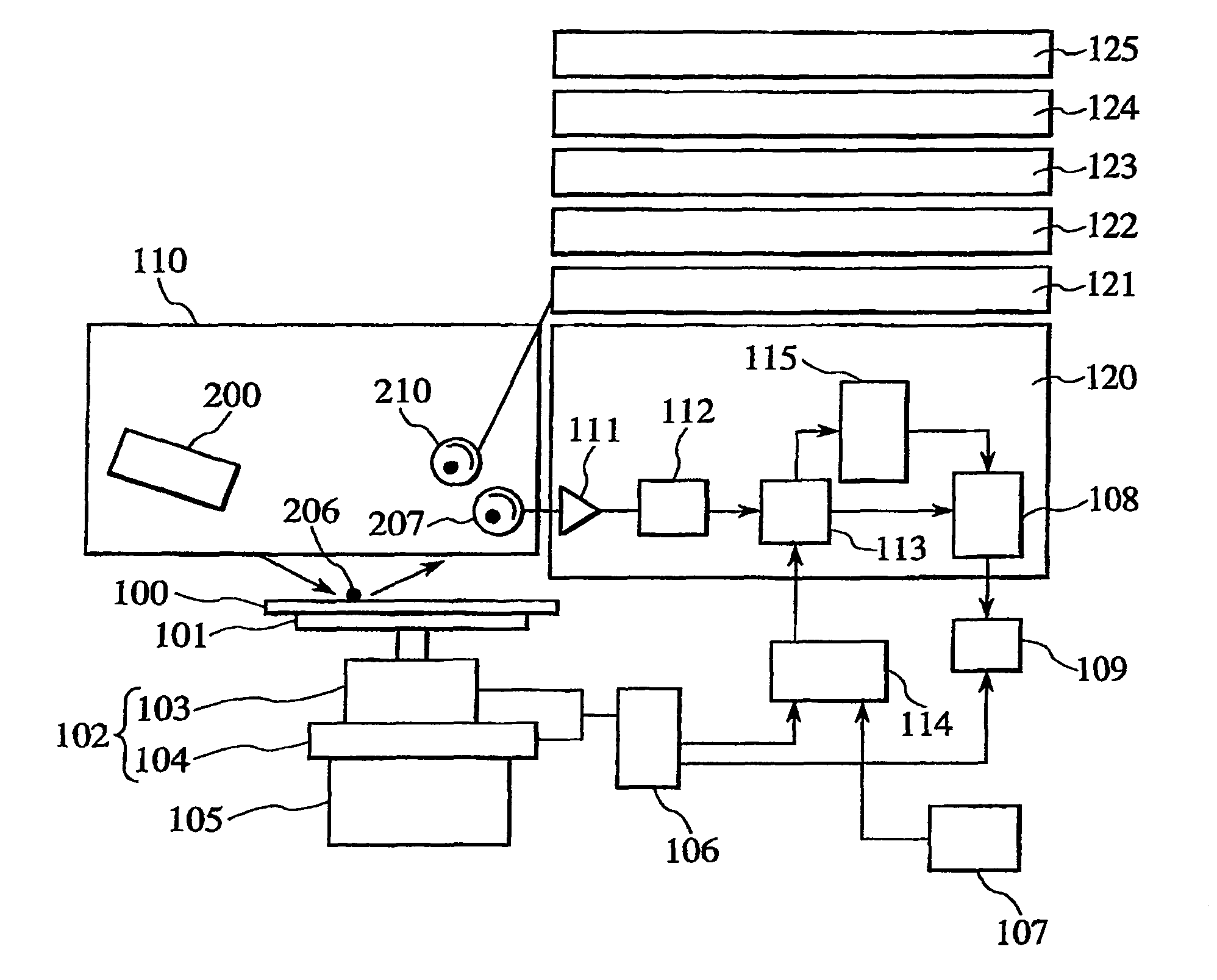
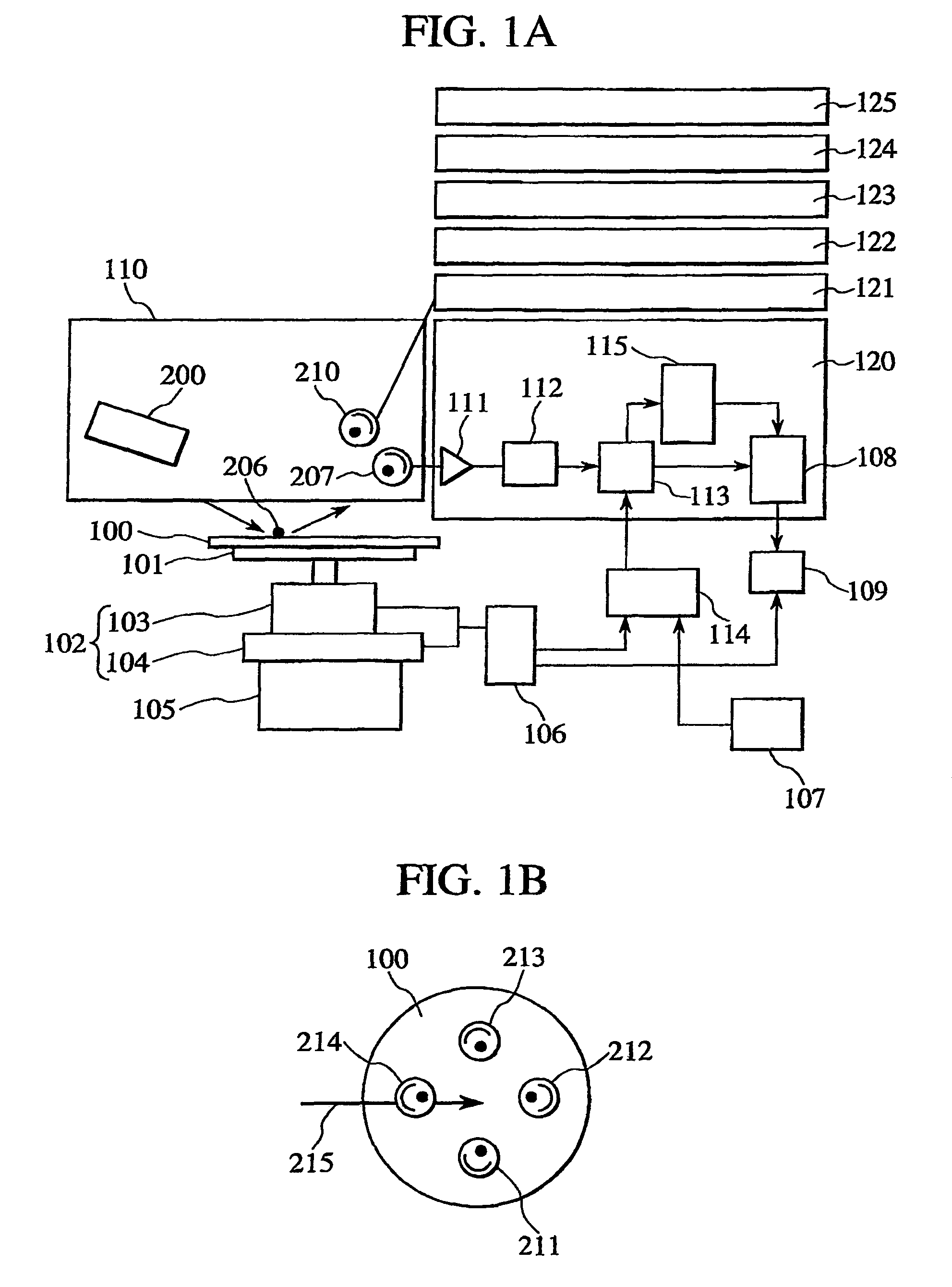
[0023]FIG. 1A is a diagram showing a defect (foreign material) inspection apparatus using a method for detecting a defect or a foreign material according to an embodiment of the present invention. FIG. 1B is a plan view of a semiconductor wafer 100.

[0024]The semiconductor wafer 100 (that is an object to be inspected) is vacuum sucked by a chuck 101. The chuck 101 is placed on a movable stage 102 for moving the object to be inspected. The stage 102 is constituted by a rotation stage 103 and a translational stage 104. The stage 102 is placed on a Z stage 105. The rotation stage 103 performs a rotational motion θ, while the translational stage 104 performs a translational motion r.

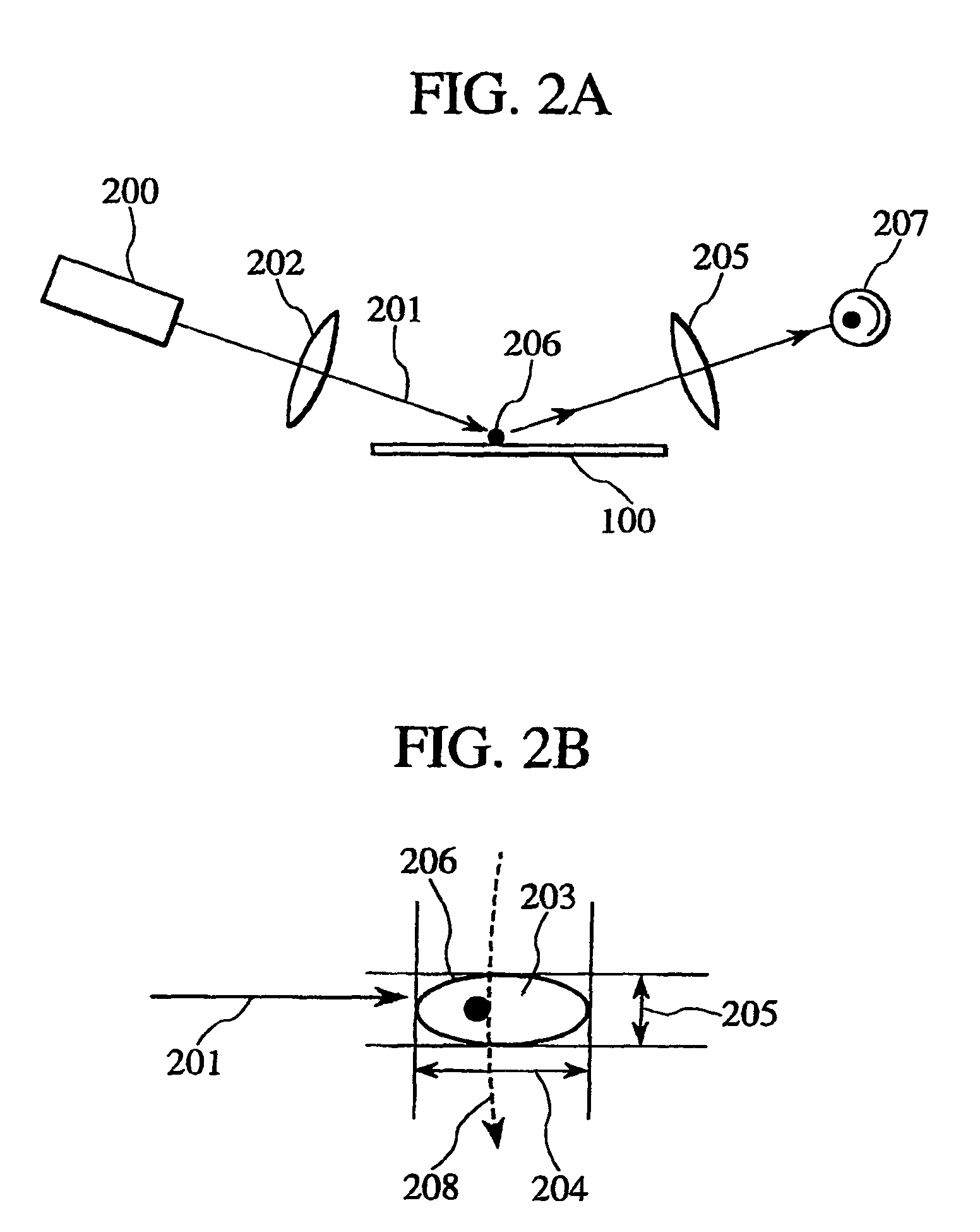
[0025]FIG. 2A shows an illumination detection optical system arranged above the semiconductor wafer 100. FIG. 2B is a plan view of the semiconductor wafer 100.

[0026]An illumination light source 200 uses a laser light source. The illumination light source 200 emits a beam 201. The beam 201 is incident on a len...


PUM

PropertyMeasurementUnit
electricaaaaaaaaaa
haze frequencyaaaaaaaaaa
frequencyaaaaaaaaaa

Abstract

Reflected light caused by the state of the surface of a wafer, a foreign material or a defect is superimposed on a haze frequency component caused by the type and thickness of a film or a surface irregularity. It has therefore been difficult to accurately measure the haze frequency component by use of a fixed threshold value. In order to detect a haze frequency component caused by a haze present on the surface of an object to be inspected, light propagating from the object to be inspected is detected and converted into an electric signal. The electric signal is sampled at a predetermined sampling time interval and converted into digital data. A frequency component caused by a foreign material, a defect or the like is separated from the digital data to ensure that a haze frequency component is selected. The haze frequency component is caused by a stain attached to the surface of the wafer, hazy tarnish, a surface irregularity or the like.

Description

BACKGROUND OF THE INVENTION[0001]1. Field of the Invention[0002]The present invention relates to an apparatus and method for inspection of the surface of an object to be inspected.[0003]2. Description of the Related Art[0004]Conventionally, as described in JP-A-63-143830, since various defects are present on a silicon wafer plate (that is a semiconductor material) and cause a reduction in the quality of an integrated circuit manufactured, the silicon wafer plate is inspected by a plate defect inspection apparatus.[0005]Recently, since the density of an integrated circuit has been increased, and rigorous inspection has been carried out on defects, it is necessary that the types of defects be discriminated and detected.[0006]Many types of defects may be present on a wafer plate. One type of the defects is a haze such as a stain attached to the surface of the plate, hazy tarnish, or a surface irregularity. It is requested to detect those defects.[0007]The haze is distributed in a relat...

Claims


Application Information

Patent Timeline
Patent Type & Authority Patents(United States)
IPC IPC(8): G01N21/88
CPCG01N21/9501G01N2021/8896G01N2021/8928
Inventor TAKAHASHI, KAZUOJINGU, TAKAHIRO
Owner HITACHI HIGH-TECH CORP
Learn More