Method for providing an efficient thermal transfer through a printed circuit board

a technology of printed circuit board and thermal transfer, which is applied in the direction of printed circuit, cable/conductor manufacturing, conductive pattern formation, etc., can solve the problems of unique thermal problems in the design of printed circuit board, designers may be forced to use more expensive metal core boards

Inactive Publication Date: 2012-02-14
HONEYWELL INT INC
View PDF13 Cites 8 Cited by
  • Summary
  • Abstract
  • Description
  • Claims
  • Application Information

AI Technical Summary

Problems solved by technology

Surface mount device (SMD) and thru-hole component packages that dissipate high power levels, such as Light Emitting Diodes (LEDs), present unique thermal problems in the design of printed circuit boards (PCBs).
The challenge at the next level of design is sinking the heat away from the component to a metal heat sink.
When designing PCBs to include devices such as surface-mounted LEDs, designers may be forced to use more expensive metal core boards in order to dissipate the heat generated by the LEDs.

Method used


Image

  • Method for providing an efficient thermal transfer through a printed circuit board
  • Method for providing an efficient thermal transfer through a printed circuit board
  • Method for providing an efficient thermal transfer through a printed circuit board

Examples


Embodiment Construction

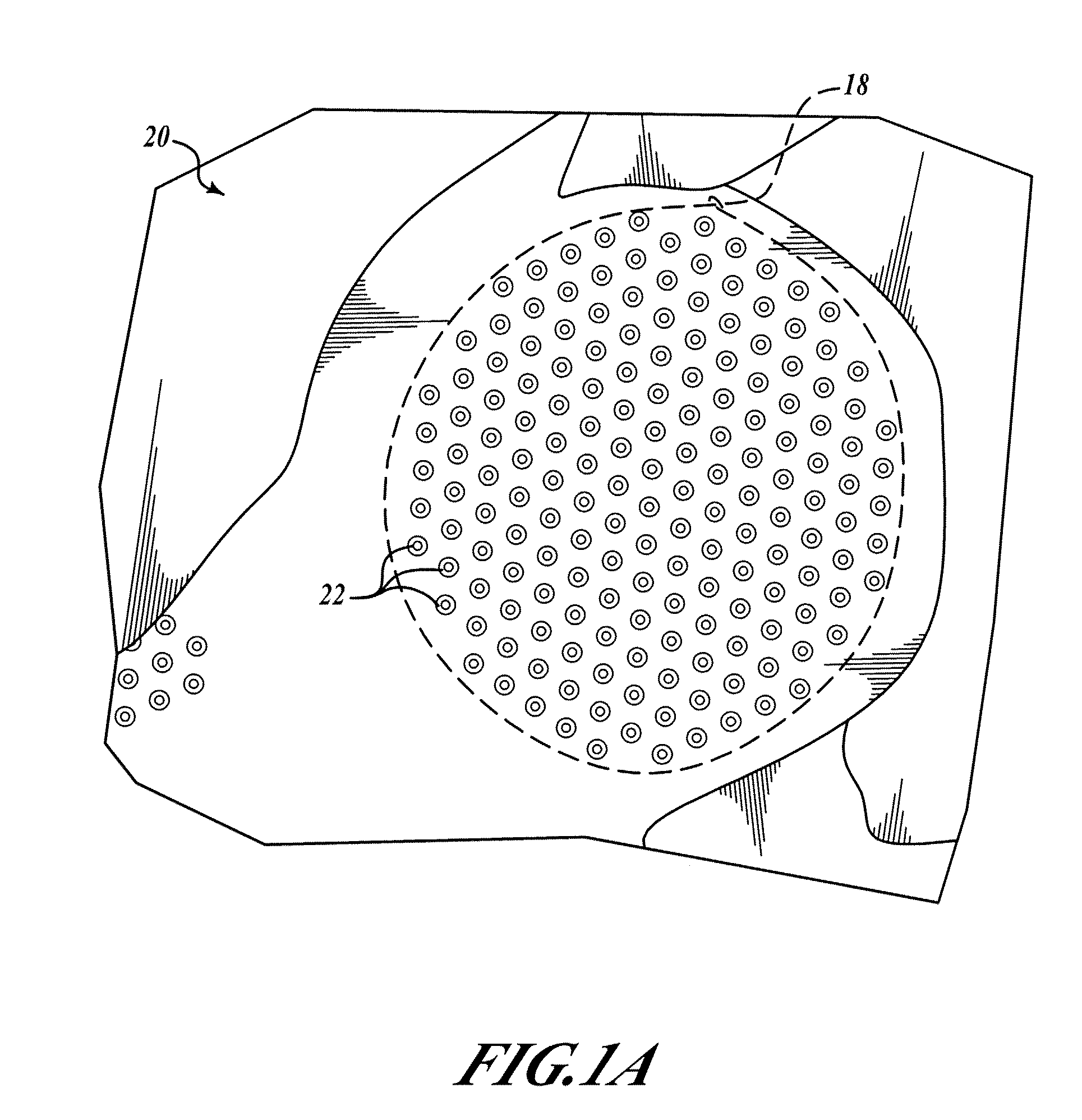
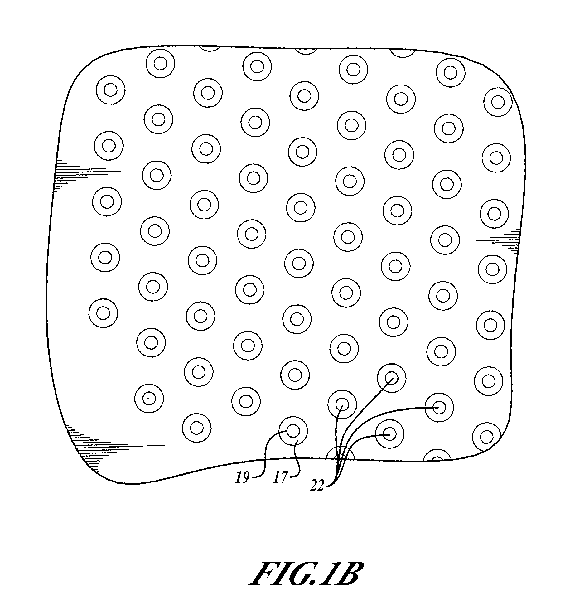
[0011]FIG. 1A shows a top view of a portion of a printed circuit board (PCB) 20, including a slug pad 18 and multiple copper-lined and non-conductive material filled vias (or holes) 22. The slug pad 18 includes copper and covers the vias 22. The pad 18 provides a thermally conductive path to all of the vias 22 and helps to promote an even distribution of thermal flow through the area of the PCB 20 covered by the pad 18. FIG. 1B shows a magnified view of the vias 22 of FIG. 1A. The vias 22 include a copper lining 17 (which may include more than one layer of copper) and a filler material 19. FIG. 1C shows a side cross-sectional view of a PCB 20 with vias 22.

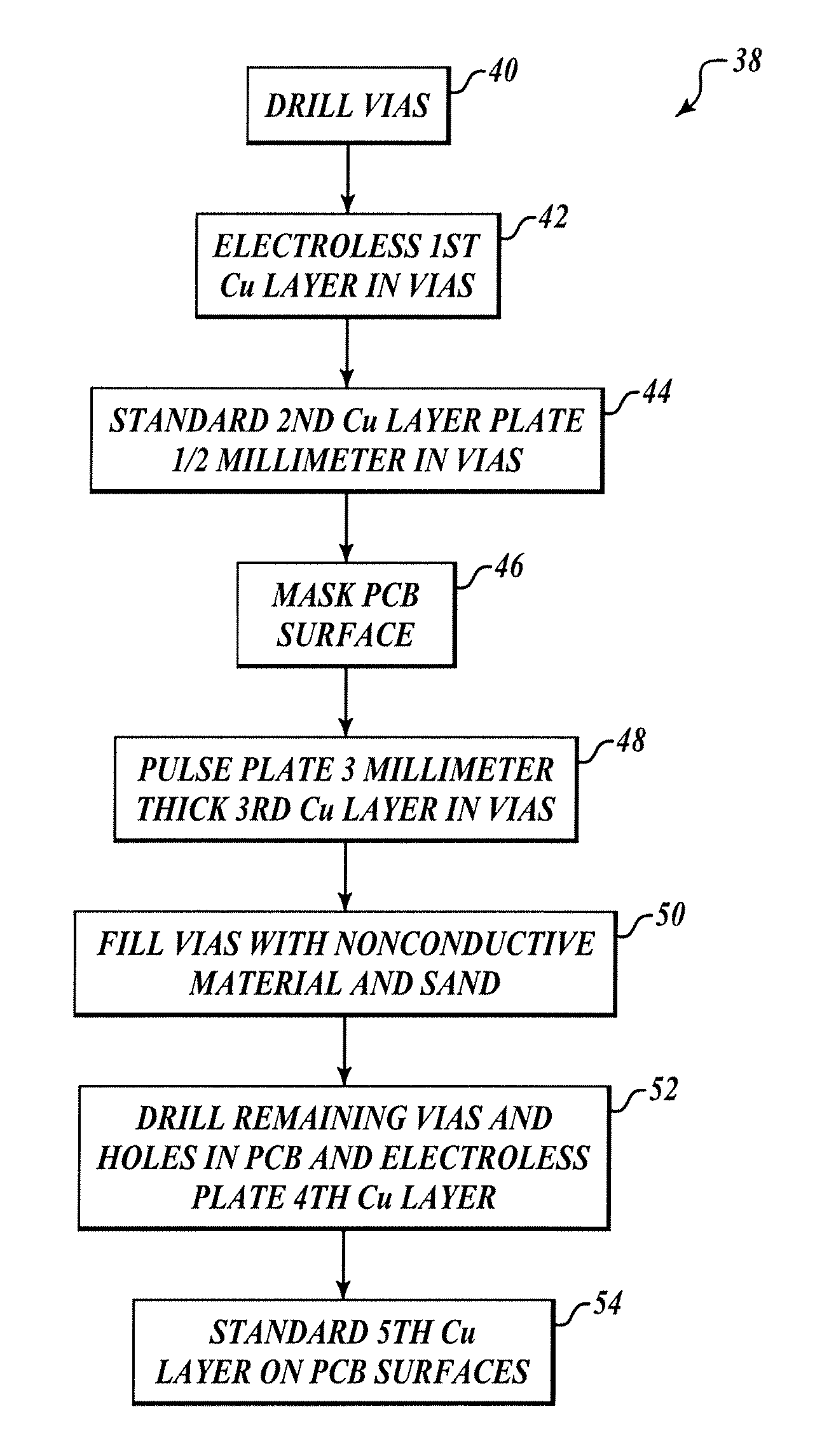
[0012]FIG. 2 shows a PCB 20, which may be made from FR4 circuit board material, according to the present invention with a top surface 21 and a bottom surface 23 after drilling one or more vias 22 through the board 20. Vias 22 are drilled in the area of the PCB 20 where a surface mount device (not shown) is to be mounted. One presen...


PUM

PropertyMeasurementUnit
thickaaaaaaaaaa
areaaaaaaaaaaa
thickaaaaaaaaaa

Abstract

A method of heat sinking a surface mount device (SMD) component. In an example method through holes are formed in a printed circuit board (PCB), a first copper layer is electroless plated in the holes, a second copper layer is standard plated in the holes and surrounding surfaces of the PCB, a third copper layer is masked and pulse plated in the holes, the holes are filled with non-conductive material and then is sanded flush with the second copper layer. A fourth copper layer electroless plated on the PCB over the area of the holes, a fifth copper layer (or pad) plated on the PCB over the area of the holes, and a surface mount device is attached to the fifth copper layer.

Description

BACKGROUND OF THE INVENTION[0001]Surface mount device (SMD) and thru-hole component packages that dissipate high power levels, such as Light Emitting Diodes (LEDs), present unique thermal problems in the design of printed circuit boards (PCBs). Component manufacturers provide tabs, slugs, or other metal protrusions from their packages to help remove the heat from the junction of the device. The challenge at the next level of design is sinking the heat away from the component to a metal heat sink.[0002]When designing PCBs to include devices such as surface-mounted LEDs, designers may be forced to use more expensive metal core boards in order to dissipate the heat generated by the LEDs. What is needed is a method of manufacturing a non-metal core board with equivalent or superior thermal performance to be able to sink away the large amounts of heat associated with SMD components such as LEDs with high power levels.SUMMARY OF THE INVENTION[0003]The present invention uses via in pad tec...

Claims


Application Information

Patent Timeline
Patent Type & Authority Patents(United States)
IPC IPC(8): H01K3/10
CPCH05K1/0206H05K1/113H05K3/108H05K3/243H05K3/423Y10T29/49155H05K2201/0347H05K2201/0959H05K2203/025H05K2203/1492Y10T29/49165H05K3/426
Inventor TULLIDGE, LEE H.DE OTO, LEONARDLARSON, TIMO'KEEFE, PATRICKGERTZ, HERB
Owner HONEYWELL INT INC
Why Eureka
Try Eureka