Thin film photovoltaic module with contoured deairing substrate

a photovoltaic module and substrate technology, applied in the direction of insulated conductors/cables, cables, insulation conductors, etc., can solve the problems of difficult to obtain an acceptable lamination of polymeric layers, difficult to use products, and relatively expensive fabrication of designs, etc., to facilitate the deairing and lamination of modules, reduce or eliminate the amount of trapped air

Inactive Publication Date: 2012-02-28
SOLUTIA INC
View PDF23 Cites 1 Cited by
  • Summary
  • Abstract
  • Description
  • Claims
  • Application Information

AI Technical Summary

Benefits of technology

[0008]The present invention provides a thin film photovoltaic module that has a protective substrate, such as glass, that has been contoured to define a space that allows air to avoid entrapment by a bus bar on the thin film photovoltaic device. The contouring of the protective substrate greatly facilitates the deairing and lamination of the module because it reduces or eliminates the amount of trapped air during lamination.
[0009]Photovoltaic modules of the present invention can be processed with a minimum of waste caused by deairing and related lamination problems.

Problems solved by technology

This conventional design, while useful, is relatively expensive to fabricate and difficult to employ in non-standard applications.
One particularly persistent problem that has been encountered in the manufacture of thin film photovoltaic modules is the difficulty in obtaining an acceptable lamination of the polymeric layer, which is typically provided in sheet form, when a bus bar is present.
A failure to properly de-air the bus bar region of the module during fabrication frequently results in an unusable product.

Method used


Image

  • Thin film photovoltaic module with contoured deairing substrate
  • Thin film photovoltaic module with contoured deairing substrate

Examples


Embodiment Construction

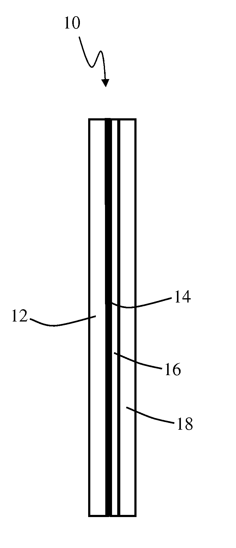
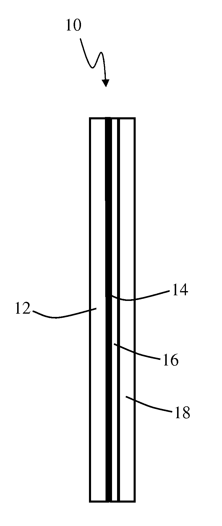
[0011]Thin film photovoltaic devices of the present invention utilize protective substrates that have a surface that has been modified from a planar state to one having contours formed thereon that serve to direct air away from entrapment points near projecting bus bars of an underlying photovoltaic device.

[0012]A schematic representation of the general configuration of a thin film photovoltaic module is shown in FIG. 1 generally at 10. As shown in FIG. 1, a thin film photovoltaic device 14 is formed on a base substrate 12, which can be, for example, glass or plastic. A protective substrate 18 is bound to the photovoltaic device 14 with a polymer layer 16. As described in more detail below, the polymer layer 16 can comprise any suitable polymer.

[0013]Previous attempts to provide a polymer layer that acceptably seals the photovoltaic module have included using polymeric materials that have relatively high flow, using relatively thick sheets of polymer, using higher lamination pressur...


PUM

PropertyMeasurementUnit
widthaaaaaaaaaa
widthaaaaaaaaaa
depthaaaaaaaaaa

Abstract

The present invention provides a thin film photovoltaic module that has a protective substrate, such as glass, that has been contoured to define a space that allows air to avoid entrapment by a bus bar on the thin film photovoltaic device. The contouring of the protective substrate greatly facilitates the deairing and lamination of the module because it reduces or eliminates the amount of trapped air during lamination.Photovoltaic modules of the present invention can be processed with a minimum of waste caused by deairing and related lamination problems.

Description

FIELD OF THE INVENTION[0001]The present invention is in the field of thin film photovoltaic modules, and, specifically, the present invention is in the field of thin film photovoltaic modules incorporating a polymer layer and a photovoltaic device on a suitable thin film photovoltaic substrate.BACKGROUND[0002]There are two common types of photovoltaic (solar) modules in use today. The first type of photovoltaic module utilizes a semiconductor wafer as a substrate and the second type of photovoltaic module utilizes a thin film of semiconductor that is deposited on a suitable substrate.[0003]Semiconductor wafer type photovoltaic modules typically comprise the crystalline silicon wafers that are commonly used in various solid state electronic devices, such as computer memory chips and computer processors. This conventional design, while useful, is relatively expensive to fabricate and difficult to employ in non-standard applications.[0004]Thin film photovoltaics, on the other hand, can...

Claims


Application Information

Patent Timeline
Patent Type & Authority Patents(United States)
IPC IPC(8): H01L31/048
CPCB32B17/10036B32B17/10146B32B17/10761H01L31/048Y02E10/50
Inventor KORAN, FRANCOIS ANDRENORTON, STEPHEN JOSEPHTRAN, KHANH DUC
Owner SOLUTIA INC
Why Eureka
Try Eureka