

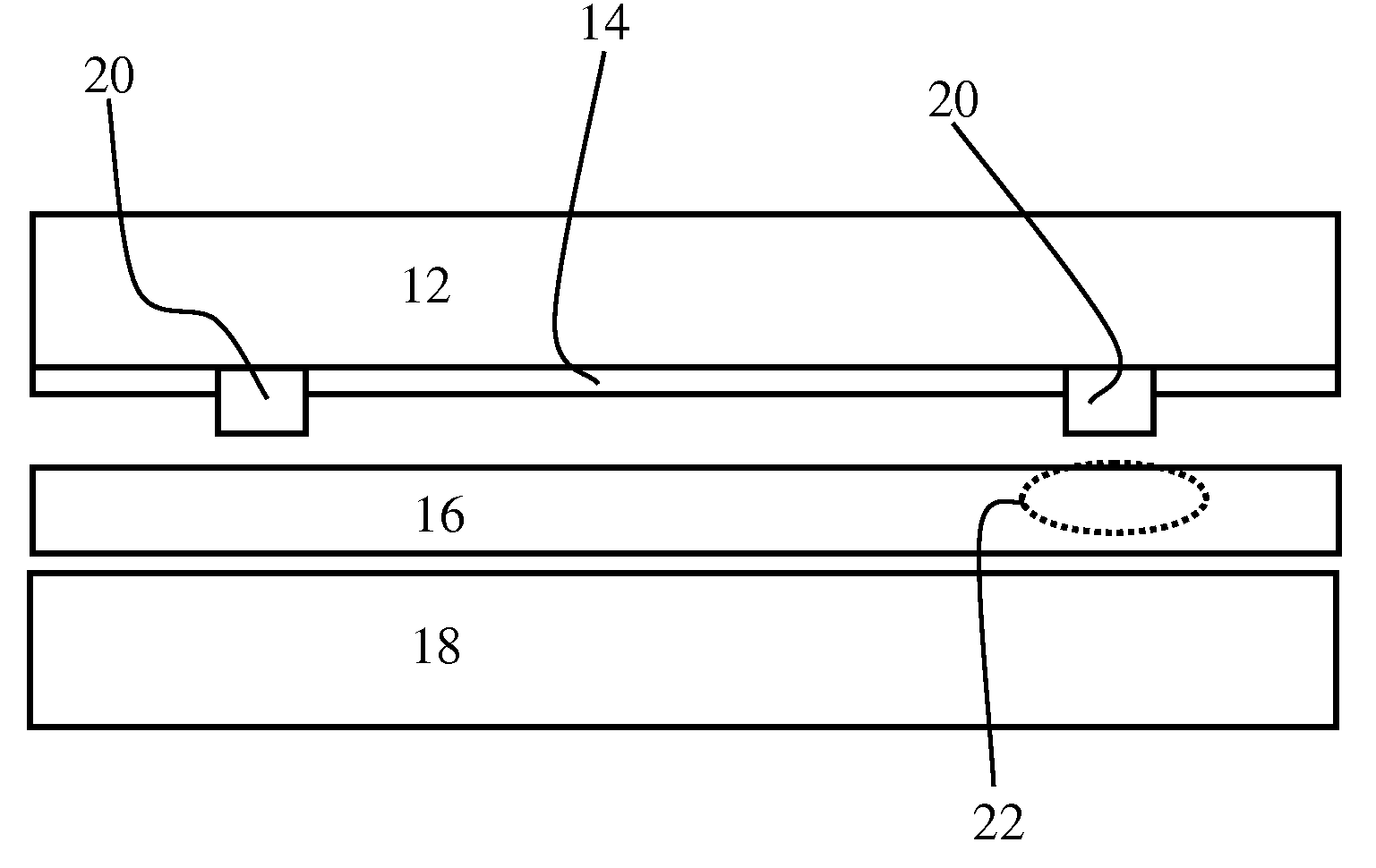
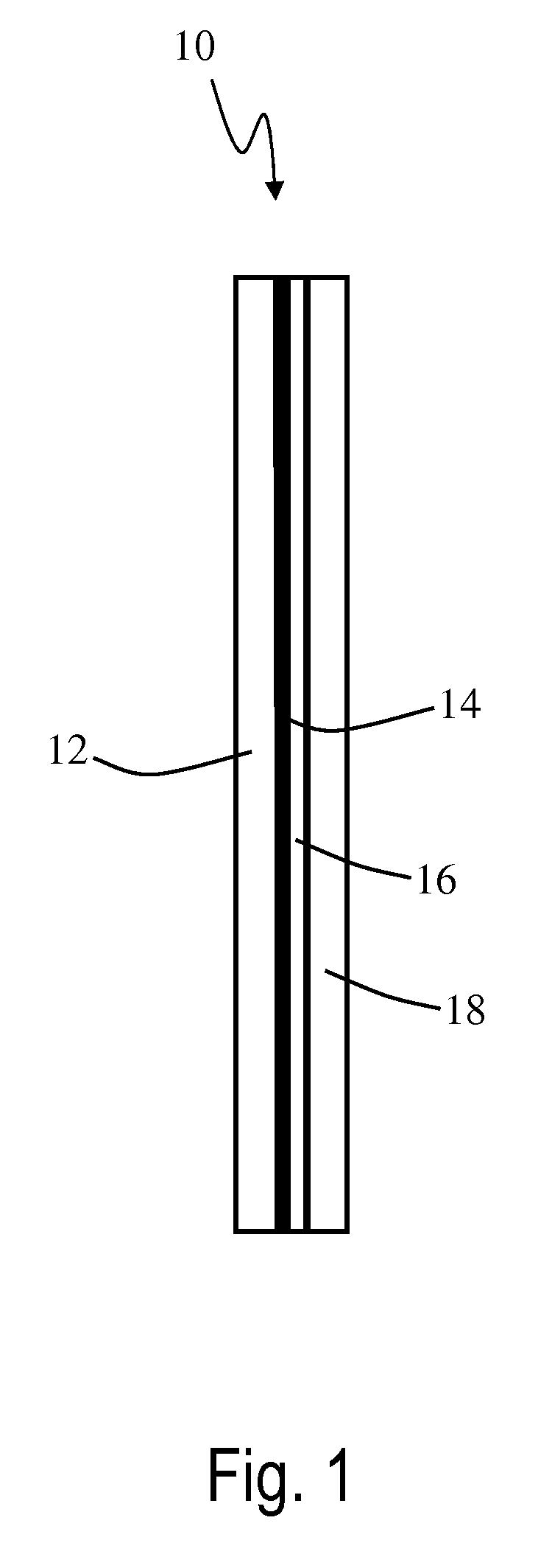
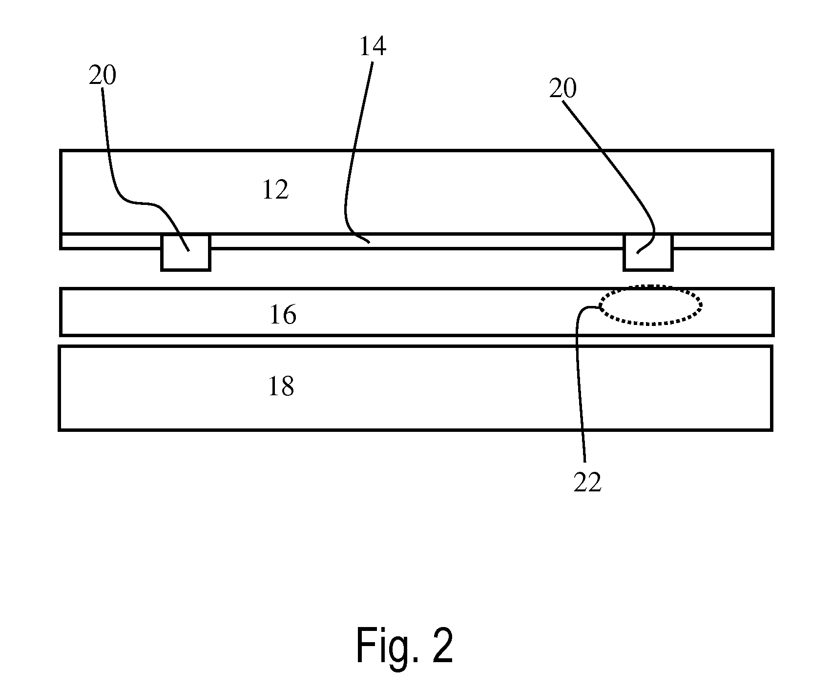
Thin Film Photovoltaic Module Having a Contoured Substrate
a technology of photovoltaic modules and contoured substrates, which is applied in the direction of layered products, pv power plants, chemical instruments and processes, etc., can solve the problems of difficult to obtain an acceptable lamination of polymeric layers, difficult to use products in non-standard applications, and relatively expensive fabrication of designs, etc., to facilitate the deairing and lamination of modules, reduce or eliminate the amount of trapped air
- Summary
- Abstract
- Description
- Claims
- Application Information
AI Technical Summary
Benefits of technology
Problems solved by technology
Method used
Image

Examples
example 1
[0062]A mock thin film photovoltaic panel with dimensions 45.72 centimeters (18″) by 53.98 centimeters (21¼″) is prepared with buss bars to approximate the critical dimensions and location of thickness step changes in typical photovoltaic panels.
[0063]A section of poly(vinyl butyral) sheet of 0.38 millimeter thickness is cut slightly larger than the size of the final photovoltaic module and is placed in an environmental chamber for approximately 12 hours at 24° C. and a relative humidity of 18%. Expected moisture content of the resulting sheet is 0.39%.
[0064]A rear protective glass layer, with a thickness of 3 millimeters, is contoured with grooves matching the location of the buss bars on the corresponding mock thin film photovoltaic panel. The depth of the machined grooves ranges from 152.4 to 203.2 microns (0.006″-0.008″), which is slightly shallower than the 203.2 micron buss bars.
[0065]The width of the machined grooves is 8 and 12 millimeters, which exceeds the respective buss ...
example 2
[0068]A mock thin film photovoltaic panel with dimensions 45.72 centimeters (18″) by 53.98 centimeters (21¼″) is prepared with buss bars to approximate the critical dimensions and location of thickness step changes in typical photovoltaic panels.
[0069]A section of poly(vinyl butyral) sheet of 0.38 millimeter thickness is cut slightly larger than the size of the final photovoltaic module and placed in an environmental chamber for approximately 12 hours at 24° C. and a relative humidity of 18%. Expected moisture content of the resulting sheet is 0.39%.
[0070]A rear protective glass layer, with a thickness of 3 millimeters, is contoured with grooves matching the location of the buss bars on the corresponding mock thin film photovoltaic panel. The depth of the machined grooves ranges from 152.4 to 203.2 microns (0.006″-0.008″), which is slightly shallower than the 203.2 micron buss bars. The width of the machined grooves is 6 and 10 millimeters, which exceeds the respective buss bar widt...
example 3
[0072]A mock thin film photovoltaic panel with dimensions 45.72 centimeters (18″) by 53.98 centimeters (21¼″) is prepared with buss bars to approximate the critical dimensions and location of thickness step changes in typical photovoltaic panels.
[0073]A section of poly(vinyl butyral) sheet of 0.38 millimeter thickness is cut slightly larger than the size of the final photovoltaic module and placed in an environmental chamber for approximately 12 hours at 24° C. and a relative humidity of 18%. Expected moisture content of the resulting sheet is 0.39%.
[0074]A rear protective glass layer, with a thickness of 3 millimeters, is contoured with grooves matching the location of the buss bars on the corresponding mock thin film photovoltaic panel. The depth of the machined grooves ranges from 76.2 to 127 microns (0.003″-0.005″), which is slightly shallower than the 203.2 micron buss bars. The width of the machined grooves is 6 and 10 millimeters, which exceeds the respective buss bar widths ...
PUM
| Property | Measurement | Unit |
|---|---|---|
| Fraction | aaaaa | aaaaa |
| Fraction | aaaaa | aaaaa |
| Thickness | aaaaa | aaaaa |
Abstract
Description
Claims
Application Information