Nitride semiconductor laser device

a laser device and nitride technology, applied in the direction of semiconductor lasers, lasers, nanotechnology, etc., can solve the problems of poor optical confinement, difficult control of optical confinement, and protective layer not having good adhesion with nitride semiconductor layer, etc., to achieve good optical confinement, improve optical output power versus input current, and long operating life

Active Publication Date: 2012-03-20
NICHIA CORP
View PDF11 Cites 2 Cited by
  • Summary
  • Abstract
  • Description
  • Claims
  • Application Information

AI Technical Summary

Benefits of technology

[0008]The present invention was conceived in view of the above circumstances, and an object of the present invention is to provide a nitride semiconductor laser device of a low threshold and having a long operating life in which good optical confinement is attained, adhesion of the protective film to both sides of the ridge is secured, the optical output power versus input current is improved.
[0010]The above aspects of the present invention can provide a nitride semiconductor laser device of a low threshold and having a long operating life in which good optical confinement is attained, adhesion of the protective film to both sides of the ridge is secured, the optical output power versus input current is improved.

Problems solved by technology

Optical confinement is easily affected by the factors other than those to be taken into consideration in the design of the devices, by the factors that may change over time such as adhesion between nitride semiconductor layer and protective film, and controlling the optical confinement has been difficult.
That is, even if a protective film having good adhesion with the nitride semiconductor layer is selected, the optical confinement may not be so good.
Also, even if a ridge is formed and a protective film is selected in consideration of the refractive index with the nitride semiconductor layer, the protective may not necessarily have good adhesion with the nitride semiconductor layer.

Method used


Image

  • Nitride semiconductor laser device
  • Nitride semiconductor laser device
  • Nitride semiconductor laser device

Examples


example 1

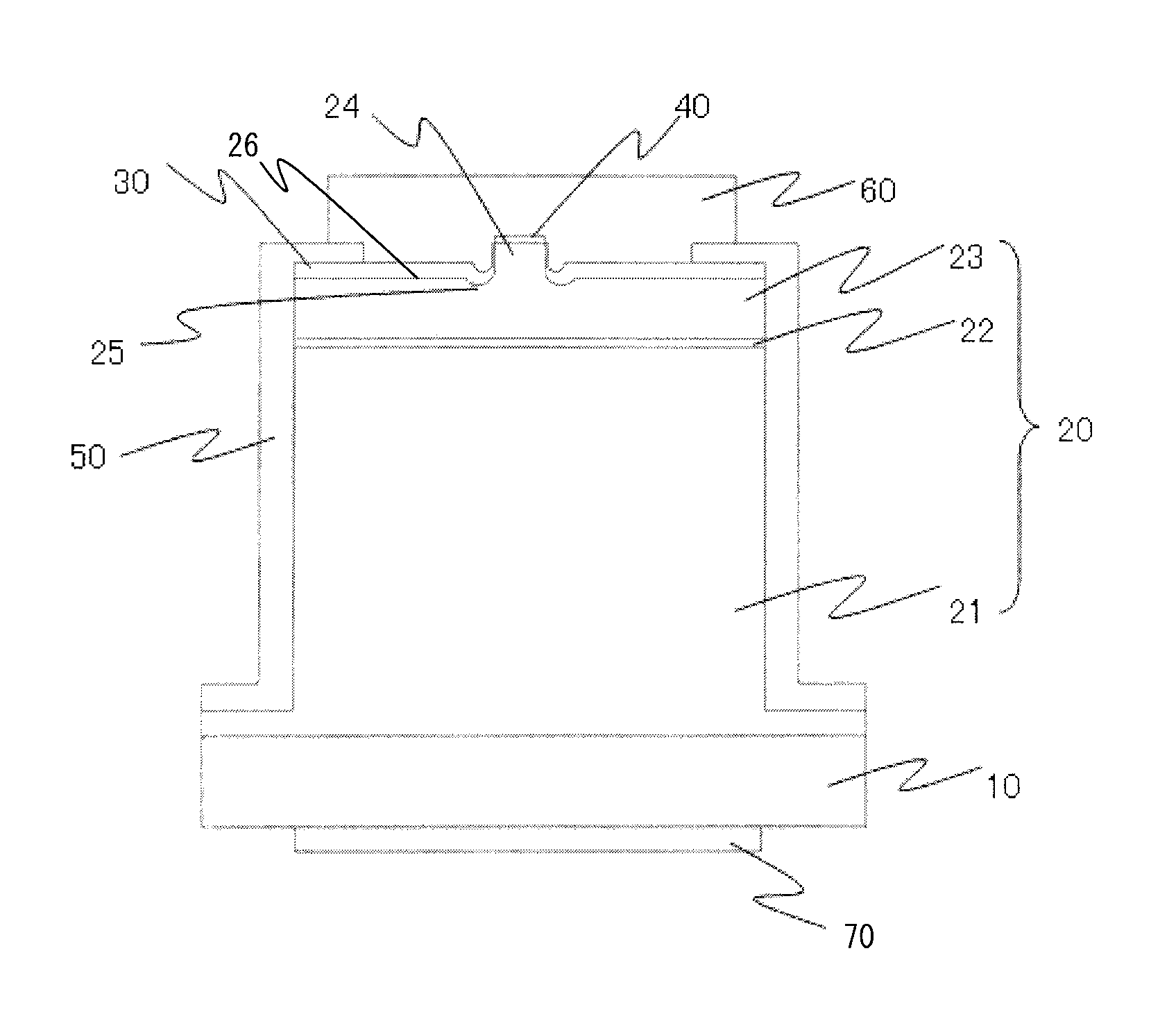
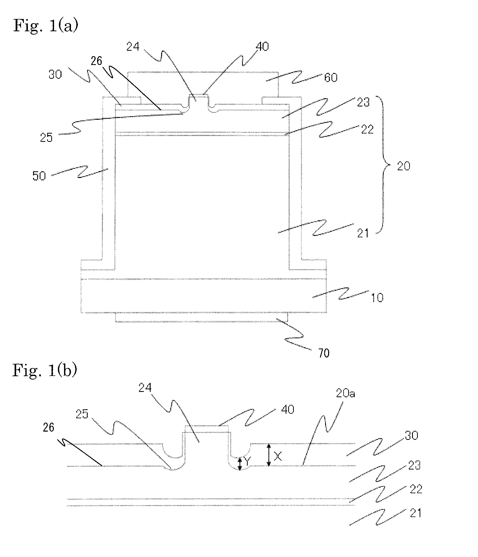
[0045]As shown in FIGS. 1(a) and (b), the nitride semiconductor laser device according to the present example is such that an n-side semiconductor layer 21, an active layer 22, and a p-side semiconductor layer 23 are formed in this order as the nitride semiconductor layer 20 over a substrate 10, and a ridge 24 is formed on the surface of the p-side semiconductor layer 23. A pair of grooves 25 is formed, whose side surfaces are surfaces continuous to side surfaces of the ridge, and an insulating film 30 is formed over from the side surfaces of the ridge 24 and the surface 20a of the nitride semiconductor layer. The bottom surface of the grooves is made with a curved surface and the insulating film is formed with a smaller thickness over the grooves than the surface of the nitride semiconductor layer. A p-side electrode 40 is formed over the ridge 24. An n-side electrode 70 is formed on the second main surface side of the substrate 10. A protective film 50 for protecting the device is...

example 2

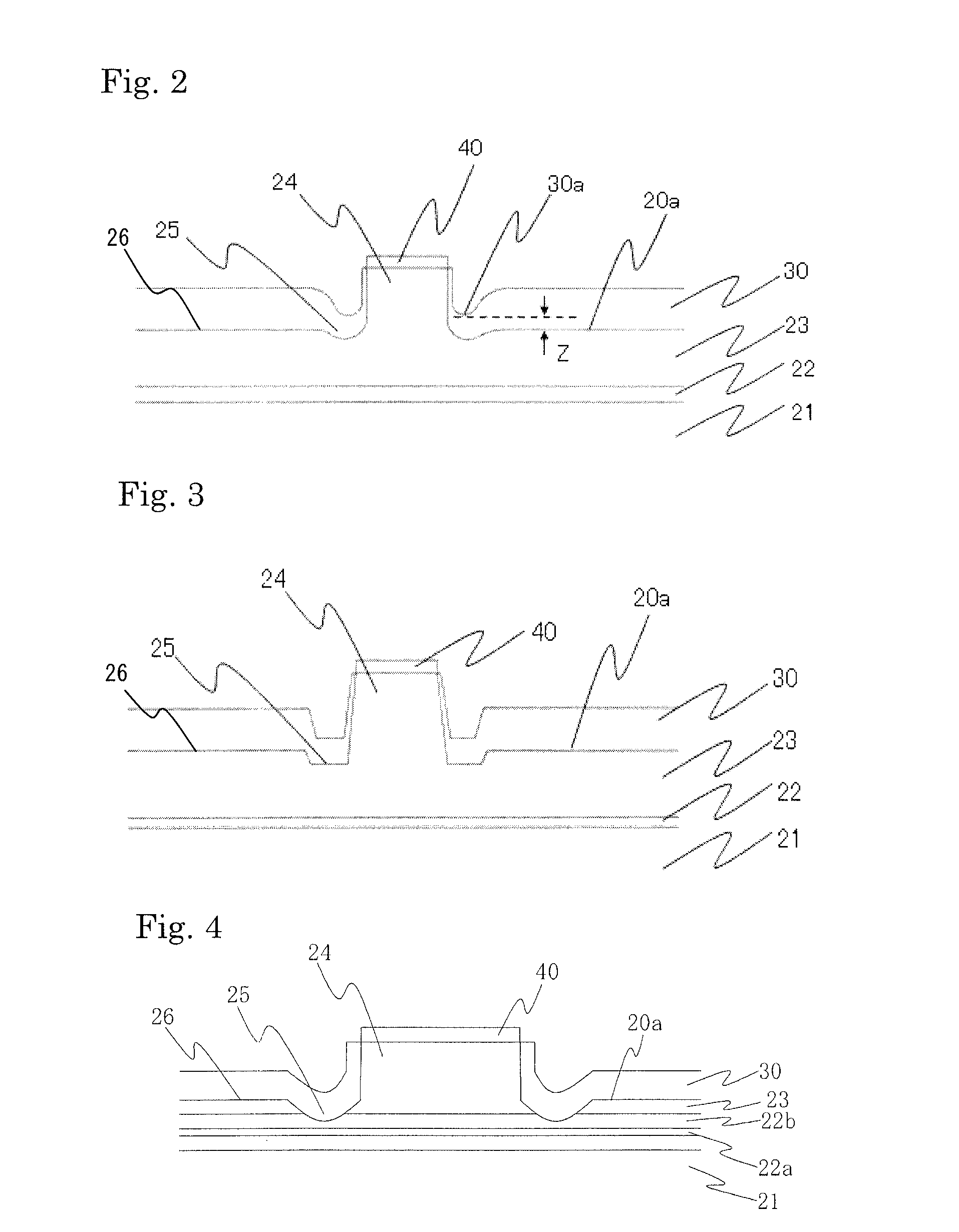
[0058]The semiconductor laser device of the present example has substantially the same configuration as in Example 1, except that the cross sectional shape of the grooves is, as shown in FIG. 2, made up of curved surfaces. According to the method of the present example, after growing the nitride semiconductor layer, grooves of 30 nm are formed by way of RIE (reactive ion etching) using a mask of the insulating film made of SiO2 which is formed as in Example 1. Then, etching of 0.74 μm is carried out at a lower etching pressure to form a stripe-shaped ridge 24 of 2.0 μm in width. Other than above, the nitride semiconductor laser device can be manufactured in substantially the same manner as in Example 1. Thus, the ridge is formed retaining the shape of the previously formed grooves, so that the grooves 25 having a cross sectional shape made up of curved surfaces are formed. With the nitride semiconductor laser devices of the present example, approximately the same effects as in Examp...

example 3

[0059]The semiconductor laser device according to the present example has substantially the same configuration as in Example 2, except the method of forming the grooves. In the present example, after forming the ridge, the etching pressure is increased and the nitride semiconductor layer at both sides of the ridge is etched by 30 nm to form the grooves. Other than above, the nitride semiconductor laser device can be manufactured in substantially the same manner as in Example 2. With the nitride semiconductor laser devices of the present example, approximately the same effects as in Example 2 can be obtained.


PUM


Abstract

The nitride semiconductor laser device includes a substrate, a nitride semiconductor layer having a first nitride semiconductor layer, an active layer, and a second nitride semiconductor layer stacked in this order on the substrate, and a ridge provided on a surface of the nitride semiconductor layer. The surface of the nitride semiconductor layer includes a generally flat part and first and second grooves which extend along the ridge in a resonator direction, the first groove being formed continuous to a first side surface of the ridge, the second groove being formed continuous to a second side surface of the ridge which is opposite to the first side surface.

Description

CROSS-REFERENCE TO THE RELATED APPLICATIONS[0001]This application claims priority to Japanese Patent Application Nos. 2009-45398 and 2010-23003 filed on Feb. 27, 2009 and Feb. 4, 2010 respectively. The entire disclosures of Japanese Patent Application Nos. 2009-45398 and 2010-23003 are hereby incorporated herein by reference.BACKGROUND OF THE INVENTION[0002]1. Field of the Invention[0003]The present invention relates to a nitride semiconductor laser device, and more particularly relates to a nitride semiconductor laser device having a ridge waveguide structure.[0004]2. Description of the Related Art[0005]A nitride semiconductor is made of a compound semiconductor including InxAlyGa1-x-yN (0≦x, 0≦y, 0≦x+y≦1), and requirements for a laser device using such a nitride semiconductor is increasing, for use in optical disc systems capable of recording and reproducing large-volume, high-density information such as a next-generation DVD, and for use in electric appliances such as personal co...

Claims


Application Information

Patent Timeline
Patent Type & Authority Patents(United States)
IPC IPC(8): H01S5/00
CPCB82Y20/00H01S5/22H01S5/34333H01S5/0655H01S5/222H01S2301/176
Inventor MIYOSHI, TAKASHIOKADA, TAKESHI
Owner NICHIA CORP
Why Eureka
Try Eureka