Laser diode with improved heat dissipation

a laser diode and heat dissipation technology, applied in the field of semiconductor laser diodes, can solve the problems of reducing the slope efficiency and maximum power output, increasing the threshold current, and reducing the efficiency of ld devices, so as to improve the heat dissipation properties and good optical confinement

Active Publication Date: 2009-09-03
SHARP FUKUYAMA LASER CO LTD
View PDF14 Cites 21 Cited by
  • Summary
  • Abstract
  • Description
  • Claims
  • Application Information

AI Technical Summary

Benefits of technology

[0007]The present invention describes a laser diode structure that simultaneously overcomes the heat dissipation and optical confinement problem. The laser diode structure includes two different insulator layers, one to maintain good optical confinement, typically located at the sides of the laser ridge, and another to improve the heat dissipation properties, typically located on the etched surfaces away from the ridge.

Problems solved by technology

However, at high power operation self-heating can affect the LD device characteristics, reducing the slope efficiency and maximum power output and increasing the threshold current.
This effect can also reduce the operating lifetime.
The poor thermal conductivity of SiO2 (k=1 W / mK) in this structure limits the heat dissipation properties of the laser diode under high power operation.
This results in self-heating which limits the device lifetime.
However, for p-side down mounted devices, the heat generated in this structure would initially still need to overcome the poor thermal conductivity SiO2 layer before reaching the high thermal conductivity protective layer.
This results in a higher dissipated power for the laser diode, which degrades the lifetime of the device.
On the other hand, insulators with low refractive index, which are beneficial for good optical confinement, are generally poor thermal conductors, and are not suitable for high power devices.

Method used


Image

  • Laser diode with improved heat dissipation
  • Laser diode with improved heat dissipation
  • Laser diode with improved heat dissipation

Examples


embodiment 1

i) EMBODIMENT 1

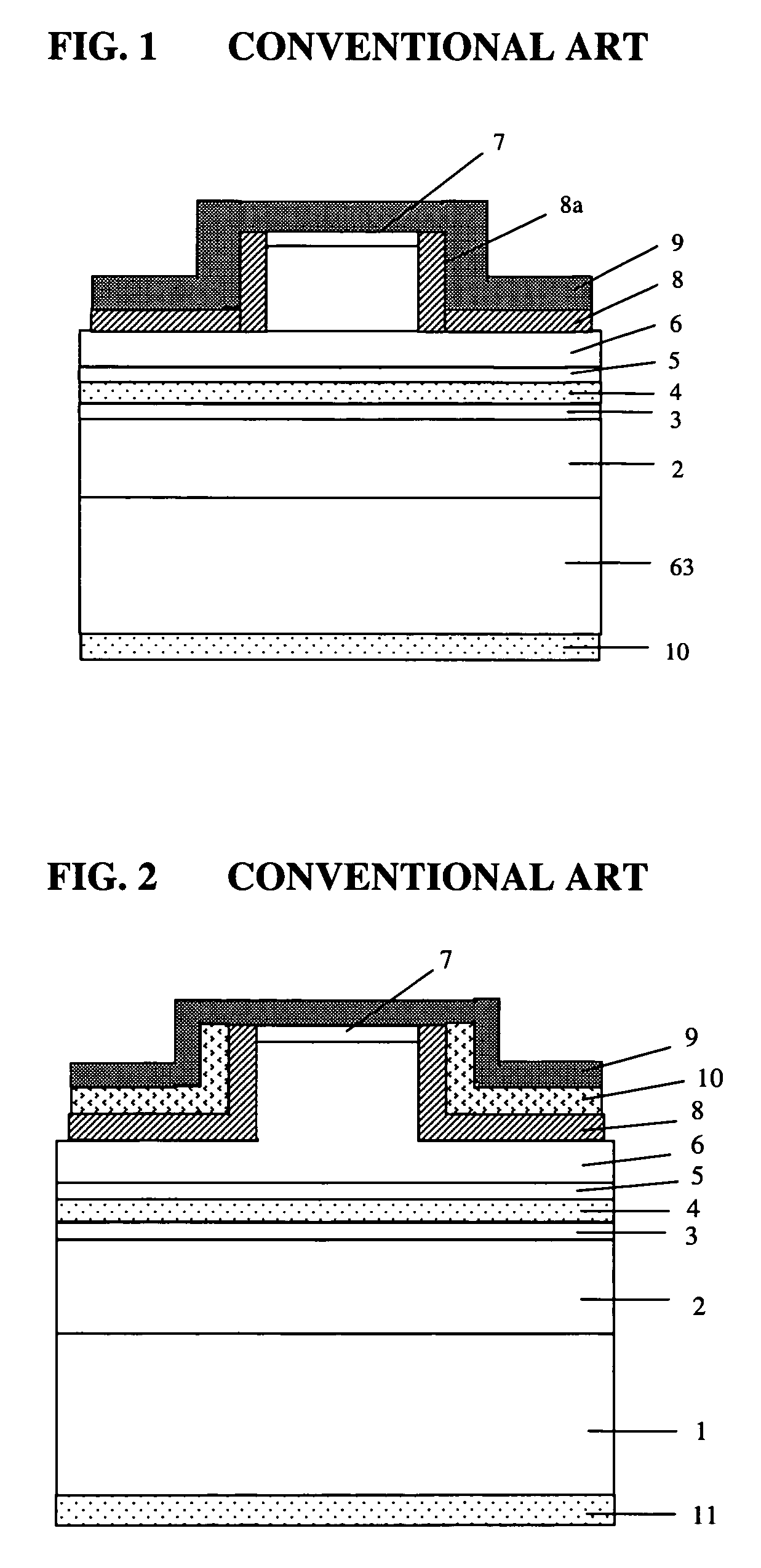
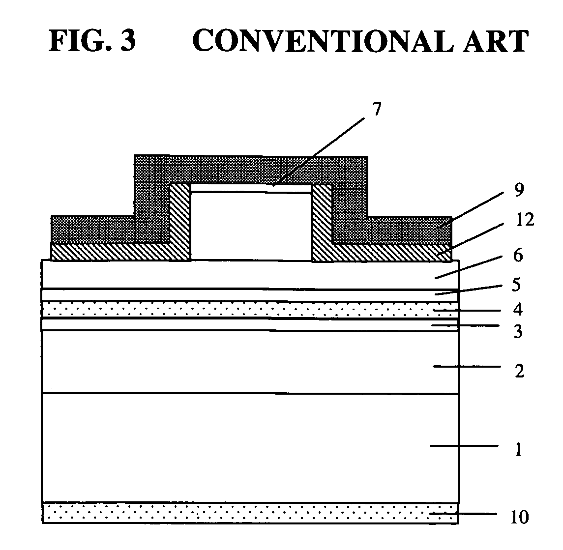
[0044]A first embodiment of a laser diode structure in accordance with the present invention is illustrated in FIG. 4A. Referring to FIG. 4A, the laser diode structure includes a substrate 50 (such as n-type GaN substrate), followed by an n-type lower cladding layer 51, an n-type lower waveguide layer 52, an active layer 53, a p-type upper waveguide layer 54, a p-type upper cladding layer 55, and a p-type contact layer 56. The cladding layers are formed by material having a lower refractive index than the waveguide layers, and the waveguide layers have a lower refractive index than the active layer. The active layer 53 may consist of a single or multiple-quantum well structure. It is preferable that a thin AlxGa1-xN blocking layer is inserted at one or both ends of the active layer to reduce carrier leakage into the waveguide layers. Electrical contact is made via the p-type electrode layer 57 and the n-type electrode layer 59. A low refractive index insulator (i.e., ...

embodiment 2

ii) EMBODIMENT 2

[0049]According to this embodiment, the structure in FIG. 4A can be modified and improved to the structure shown in FIG. 5B. FIG. 5A shows the overlap of the optical mode with the low refractive index SiO2 insulator 61a occurs mainly at the bottom of the ridge. Therefore, good optical mode confinement can still be achieved by having the SiO2 layer only at the bottom region of the ridge sidewalls 61b. A high thermal conductivity insulator (i.e. AlN) can then replace the SiO2 layer at the top region of the ridge sidewalls 63a, thus allowing better heat dissipation through the top of the ridge, as shown in FIG. 5B. In FIG. 5C, the simulated L-I characteristics and active region temperature is shown for the conventional SiO2-only structure (FIG. 1) and the invention structure, as a function of different SiO2 thickness at the ridge sidewalls. In the simulation, the mesa height of the ridge sidewall is fixed at 500 nm, hence 500 nm-SiO2 refers to the insulator thickness co...

embodiment 3

iii) EMBODIMENT 3

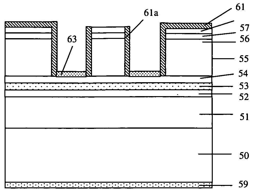
[0050]According to this embodiment, a reverse structure is also proposed, and is shown in FIG. 6A. For this structure, the high thermal conductivity insulator layer 63 is formed at the ridge sidewalls while the low refractive index insulator layer 61 is formed at the etched surfaces. FIG. 6B and FIG. 6C show the simulated active region temperature profile in Kelvin for the reverse structure of the invention (FIG. 6C) and the conventional single layer insulator structure (FIG. 6B). FIG. 6D compares the L-I characteristics and active region temperature profile for the original invention structure, the reverse invention structure and the conventional single layer SiO2 structure. From the graphs, the reverse invention structure has a reduced active region temperature profile over the conventional structure, but is still poorer than the original invention structure. Observe that the L-I curve for the original invention structure (embodiment 1) has a much reduced thermal ...


PUM


Abstract

A laser diode structure that includes two different insulator layers, one to maintain good optical confinement, typically located at the sides of the laser ridge, and another to improve the heat dissipation properties, typically located on the etched surfaces away from the ridge.

Description

TECHNICAL FIELD[0001]The present invention relates to a semiconductor laser diode. It relates, in particular to a ridge structure laser diode comprising two different materials to effectively dissipate heat at high power operation while maintaining low threshold current. A method of manufacturing such a structure is also presented.BACKGROUND OF THE INVENTION[0002]Gallium Nitride based semiconductor laser diodes (LDs) are widely used in optical storage such as Blu-ray or high definition digital video discs (HD-DVD), as means of transferring, writing or reading data. As these devices are rapidly commercialised, there is a requirement for high power LDs, in particular for high-speed writing in these systems. However, at high power operation self-heating can affect the LD device characteristics, reducing the slope efficiency and maximum power output and increasing the threshold current. This effect can also reduce the operating lifetime. Therefore, a LD that can dissipate heat efficient...

Claims


Application Information

Patent Timeline
Patent Type & Authority Applications(United States)
IPC IPC(8): H01S5/00H01S5/223
CPCB82Y20/00H01S5/0224H01S5/024H01S5/02461H01S5/0655H01S2301/18H01S5/22H01S5/2214H01S5/2219H01S5/222H01S5/34333H01S5/2009H01S5/0234
Inventor TAN, WEI-SINBARNES, JENNIFER MARY
Owner SHARP FUKUYAMA LASER CO LTD
Why Eureka
Try Eureka