Nitride semiconductor laser element

a laser element and nitride technology, applied in the direction of lasers, semiconductor lasers, active medium materials, etc., can solve the problems of poor optical confinement and protection film may not necessarily have good adhesion with the nitride semiconductor layer, and achieve good optical confinement, good adhesion, and good adhesion.

Active Publication Date: 2008-07-03
NICHIA CORP
View PDF3 Cites 7 Cited by
  • Summary
  • Abstract
  • Description
  • Claims
  • Application Information

AI Technical Summary

Benefits of technology

[0017]forming a second film containing polycrystallines or an amorphous substance over the first film, thereby forming an insulating protective film.
[0018]With the present invention, good optical confinement is attained in a nitride semiconductor laser element, while at the same time stress can be minimized between the nitride semiconductor layer and the protective film on both

Problems solved by technology

However, even when a protective film is selected by taking the refractive index into account, this protective film may not necessarily have good adhesion with the

Method used


Image

  • Nitride semiconductor laser element
  • Nitride semiconductor laser element
  • Nitride semiconductor laser element

Examples


example 1

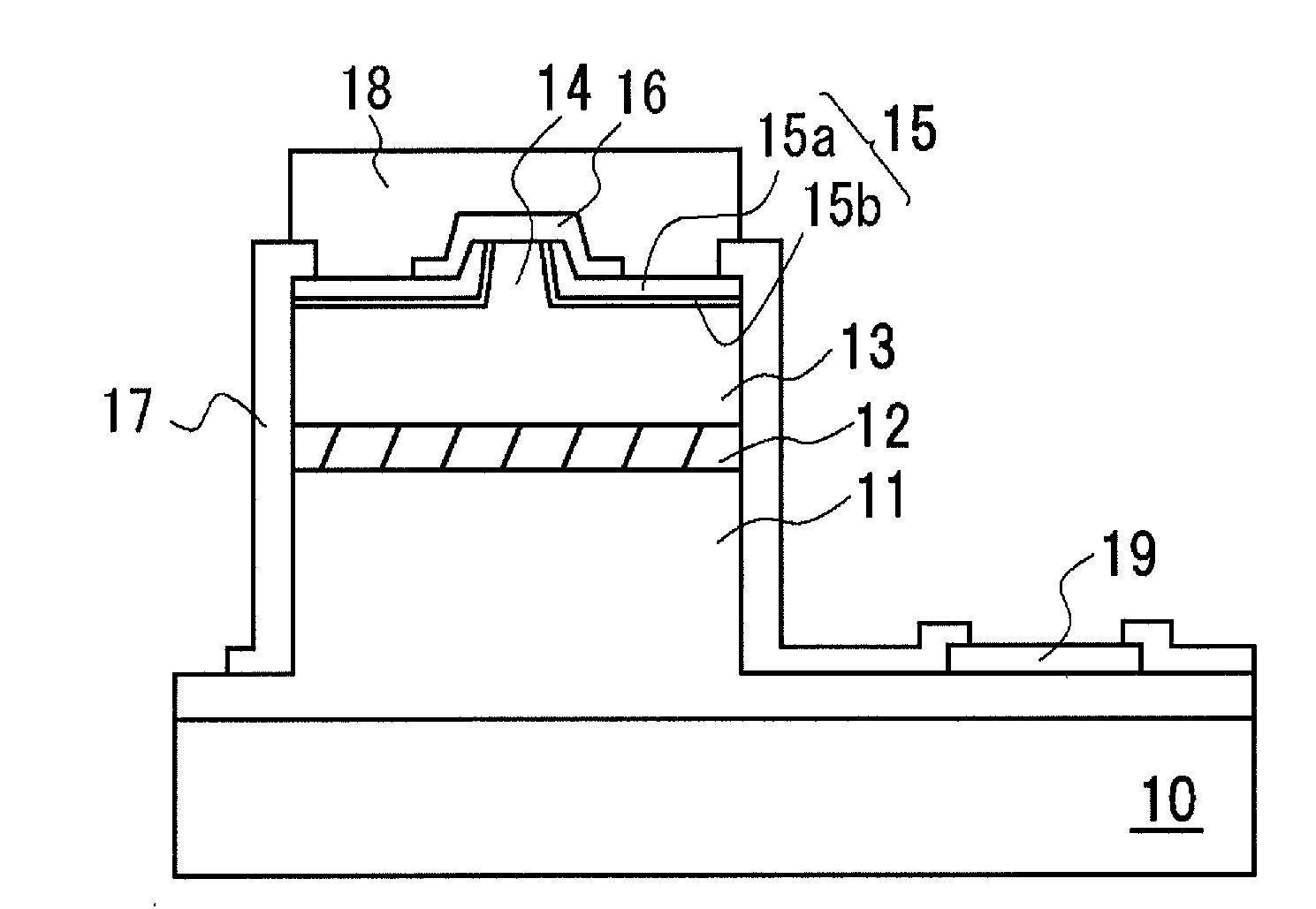
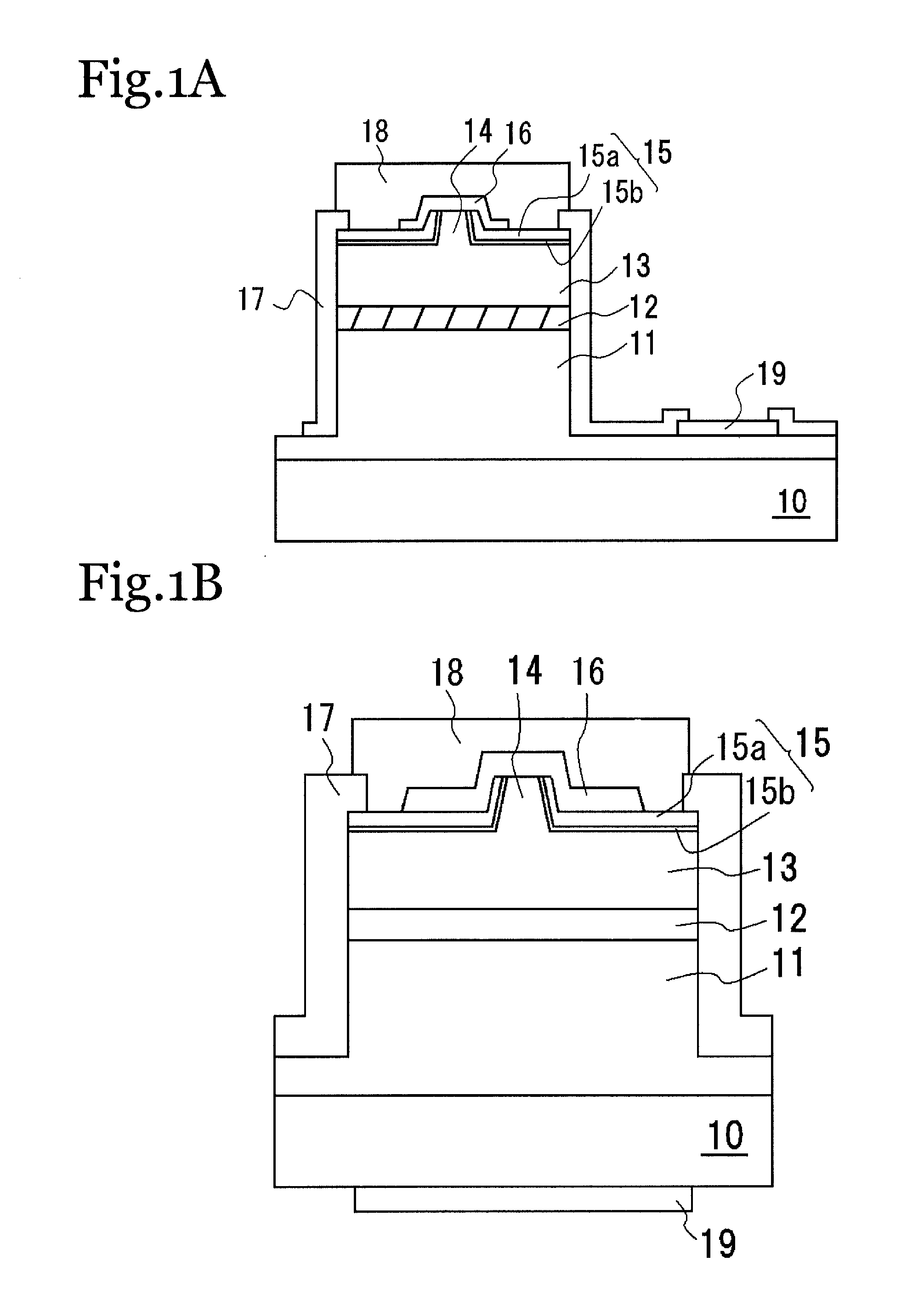
[0059]As shown in FIG. 1A, the nitride semiconductor laser element in this example is such that an n-side semiconductor layer 11, an active layer 12, and a p-side semiconductor layer 13 are formed in that order as the nitride semiconductor layer over a substrate 10, and a ridge 14 is formed on the surface of the p-side semiconductor layer 13. An insulating protective film 15 composed of a first film 15b (a monocrystalline Al2O3 film) and a second film 15a (polycrystalline or amorphous ZrO2) is formed from the side faces of the ridge 14 to the surface of the nitride semiconductor layer.

[0060]The p-side electrode 16 is formed on the top face of the ridge 14. Also, part of the nitride semiconductor layer is removed in the thickness direction, and the n-side electrode 19 is formed so as to be in contact with the n-side semiconductor laser 11. The protective film 17 for protecting the element is formed from the side faces of the nitride semiconductor layer up to the top face. The p-side ...

example 2

[0083]As shown in FIG. 1B, the semiconductor laser element in this example had substantially the same configuration as the semiconductor laser element in Example 1, except that a first film (a monocrystalline Al2O3 film) and a second film (amorphous ZrO2) were formed as an insulating protective film, and the n-side electrode 19 was formed on the second main face of the substrate 10.

[0084]First, a substrate doped with n-type impurities is readied. This substrate in which the first plane serves as the growth plane is conveyed into an MOVPE reaction vessel. A first buffer layer composed of n-Al0.02Ga0.98N doped with Si at 1.8×10¹⁸ / cm3 (2 μm thick) is grown using TMA, TMG and NH3 as the raw material gas with a silane gas for an impurity gas. Nest, the temperature is rose, a second buffer layer composed of n-In0.05Ga0.95N doped with Si at 3×10¹⁸ / cm3 (1500 Å thick) is grown using TMI, TMG, and NH3 for the raw material gas with a silane gas for an impurity gas.

[0085]Thereafter, a clad laye...

example 3

[0099]The semiconductor laser element of this example had substantially the same configuration as in Example 2, except that an insulating protective film composed of a first film (monocrystalline Al2O3 film) and second film (amorphous SiO2 film) is formed.

[0100]A condition of the first film formation is set as the same as Example 2, and a condition of the second film formation is set at a microwave power of 500 W, an RF power of 500 W, an argon flow of 20 sccm, and an oxygen flow of 6 sccm to obtain the SiO2 film (1500 Å thick).

[0101]This yielded substantially the same results as in Example 2.


PUM


Abstract

A nitride semiconductor laser element comprises a substrate, a nitride semiconductor layer that is laminated on the substrate and that has a ridge on its surface, and an electrode that is electrically connected with the nitride semiconductor layer, wherein there is provided an insulating protective film produced by forming a monocrystalline first film or a first film containing hexagonal crystals, and extending from the side faces of the ridge to the nitride semiconductor layer on both sides of the ridge, and a second film containing a polycrystalline or amorphous substance, from the nitride semiconductor layer side, in this order.

Description

BACKGROUND OF THE INVENTION[0001]1. Field of the Invention[0002]The present invention relates to a nitride semiconductor laser element, and more particularly relates to a nitride semiconductor laser element having a ridge waveguide structure.[0003]2. Background Information[0004]A nitride semiconductor is formed from a semiconductor compound containing InxAlyGa1−x−yN (0≦x, 0≦y, 0≦x+y≦1), and there has been growing demand for semiconductor laser elements that make use of this material in optical disk systems that allow large quantities of information to be recorded and reproduced in high density (such as next-generation DVDs), and in personal computers and other such electronic devices. Considerable research has therefore gone into semiconductor laser elements that make use of nitride semiconductors.[0005]Also, it is believed that semiconductor laser elements that make use of nitride semiconductors are capable of emission over a wide range of visible light wavelengths, from ultraviole...

Claims


Application Information

Patent Timeline
IPC IPC(8): H01L33/00H01L21/306
CPCB82Y20/00H01L21/0254H01L21/02576H01L21/02579H01S5/0282H01S2304/04H01S5/22H01S5/2214H01S5/3063H01S5/34333H01S5/2009
Inventor MASUI, SHINGOMORIZUMI, TOMONORI
Owner NICHIA CORP
Why Eureka
Try Eureka