Method for manufacturing oxide film having high dielectric constant, capacitor having dielectric film formed using the method, and method for manufacturing the same

a dielectric film and oxide film technology, applied in the direction of coatings, transistors, chemical vapor deposition coatings, etc., can solve the problems of difficult to apply high k-dielectric materials to the misstructure, increase leakage current, and increase so as to improve productivity and reduce the size of the used deposition apparatus , the effect of saving the time required for deposition

Inactive Publication Date: 2012-03-27
SAMSUNG ELECTRONICS CO LTD
View PDF17 Cites 13 Cited by
  • Summary
  • Abstract
  • Description
  • Claims
  • Application Information

AI Technical Summary

Benefits of technology

[0029]According to the present invention, the size of a used deposition apparatus can be reduced without degrading characteristics of high k-dielectric oxide films. Also, the time required for deposition can be saved, thus enhancing productivity.

Problems solved by technology

As the integration density of semiconductor devices, such as DRAMs, increases, manufacturing gate oxide films or capacitors using a silicon oxide (SiO2) film becomes more complicated.
However, in a metal / insulator / silicon (MIS) structure in which a lower electrode is formed of silicon (Si), since the high k-dielectric materials generally have low band offset, leakage current increases.
For this reason, it is actually difficult to apply these high k-dielectric materials to the MIS structure.
For example, costly studies are being done on a multi-layered structure in which a silicon film, an aluminum oxide (Al2O3) film, and a high k-dielectric material are sequentially stacked.
In the conventional method for manufacturing a high k-dielectric oxide film, by which an aluminum oxide film and a hafnium oxide film are sequentially stacked, the capacitance of a capacitor cannot be sufficiently increased due to low dielectric constant of the aluminum oxide film.
Also, the deposition rate of a hafnium oxide film is lower than that of an aluminum oxide film, thus lowering the productivity.
Further, as a high k-dielectric oxide film may be crystallized during a thermal treatment performed after a capacitor is completed, the leakage current may increase.

Method used


Image

  • Method for manufacturing oxide film having high dielectric constant, capacitor having dielectric film formed using the method, and method for manufacturing the same
  • Method for manufacturing oxide film having high dielectric constant, capacitor having dielectric film formed using the method, and method for manufacturing the same
  • Method for manufacturing oxide film having high dielectric constant, capacitor having dielectric film formed using the method, and method for manufacturing the same

Examples


embodiment 1

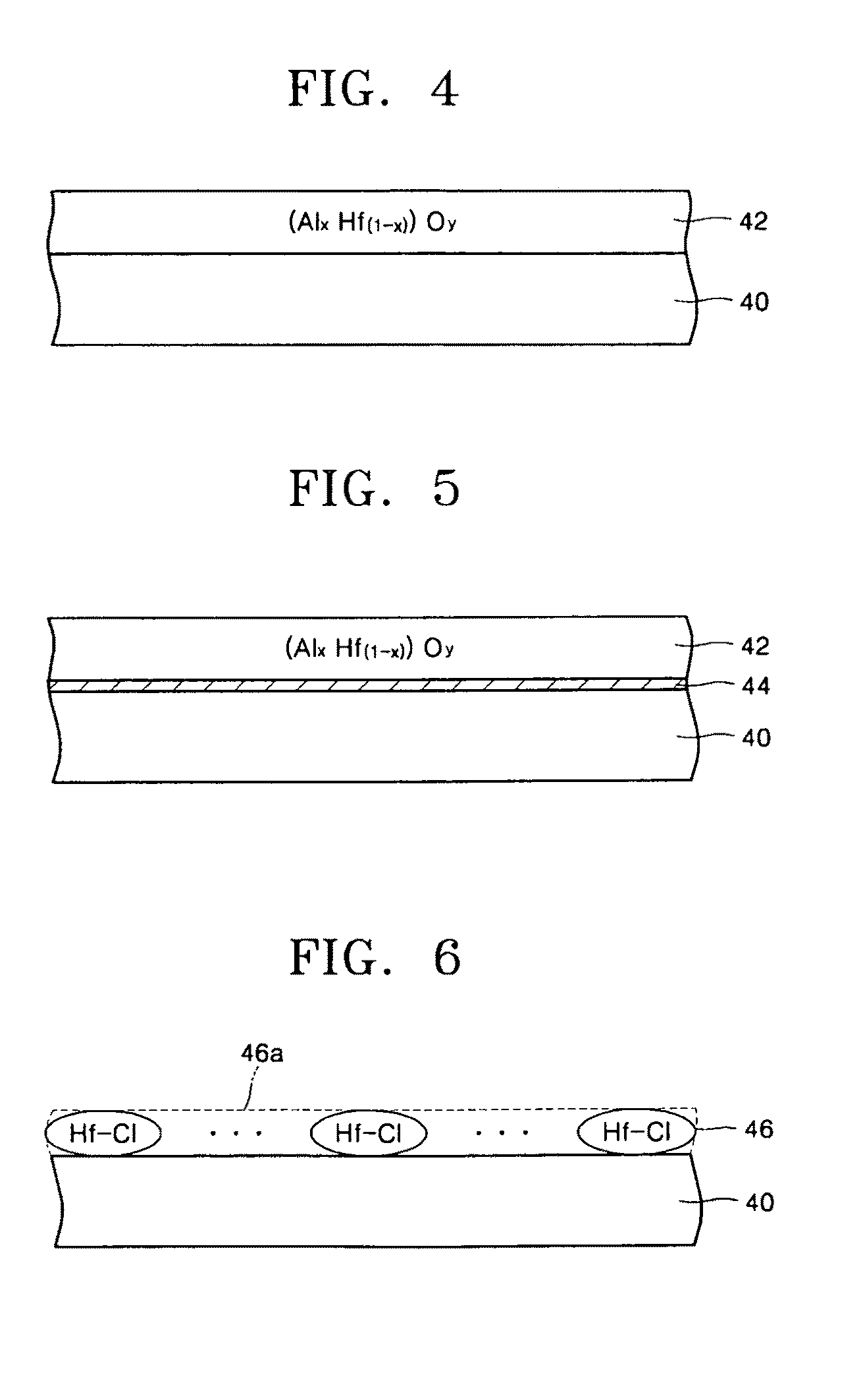
[0042]A semiconductor substrate where a high k-dielectric oxide film will be formed, e.g., a silicon substrate, is loaded on a wafer stage of an ALD apparatus (not shown). Next, a predetermined amount of a first precursor containing a first element, e.g., hafnium (Hf), is supplied to the ALD apparatus and chemisorbed on the surface of the semiconductor substrate 40, as shown in FIG. 6. The first precursor 46 is a composition of the first element and a ligand having high electronegativity, such as Cl and F. For example, the first precursor 46 is HfCl4. Part of the first precursor, which is not absorbed on the surface of the semiconductor substrate 40, is exhausted from the ALD apparatus. Afterwards, a second precursor containing a second element, e.g., aluminium (Al), which reacts with the first element of the first precursor 46, is supplied to the ALD apparatus. The second precursor is a composition of the second element and a ligand of hydrocarbon series, for example, Al(CH3)3, Al(...

embodiment 2

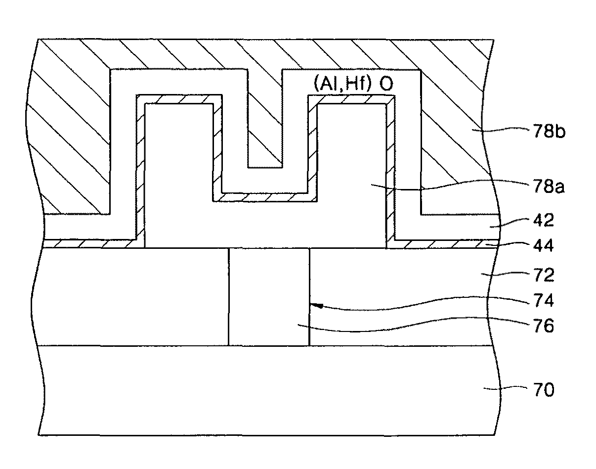
[0050]As shown in FIGS. 10 through 13, manufacturing steps in a second embodiment are the same as those in the first embodiment except that supplying the first precursor 46 through the final step are performed after an oxidation barrier film 44 is formed on the semiconductor substrate 40. The oxidation barrier film 44 is a nitride film obtained by loading the semiconductor substrate 40 in a furnace of a nitrogen atmosphere and treating it using RTP for a predetermined duration of time. The oxidation film 44 can prevent a reaction between a dielectric material and silicon, which are deposited on the semiconductor substrate 40. Thus, the dielectric constant of the dielectric material can be stably maintained. The oxidation barrier film 44 may be formed of silicon oxynitride (SiON).

[0051]Hereinafter, characteristics of the high k-dielectric oxide film according to the embodiments of the present invention will be described based on the measurement results.

[0052]FIG. 15A is a TEM showing...


PUM

PropertyMeasurementUnit
temperatureaaaaaaaaaa
leakage currentaaaaaaaaaa

Abstract

Provided are a method for manufacturing a high k-dielectric oxide film, a capacitor having a dielectric film formed using the method, and a method for manufacturing the capacitor. A high k-dielectric oxide film is manufactured by (a) loading a semiconductor substrate in an ALD apparatus, (b) depositing a reaction material having a predetermined composition rate of a first element and a second element on the semiconductor substrate, and (c) forming a first high k-dielectric oxide film having the two elements on the semiconductor substrate by oxidizing the reaction material such that the first element and the second element are simultaneously oxidized. In this method, the size of an apparatus is reduced, productivity is enhanced, and manufacturing costs are lowered. Further, the high k-dielectric oxide film exhibits high dielectric constant and low leakage current and trap density. Thus, a capacitor including the high k-dielectric oxide film as a dielectric film also exhibits low leakage current and trap density.

Description

BACKGROUND OF THE INVENTION[0001]This application claims the priority of Korean Patent Application No. 2003-15197, filed on Mar. 11, 2003, in the Korean Intellectual Property Office, the disclosure of which is incorporated herein in its entirety by reference.[0002]1. Field of the Invention[0003]The present invention relates to a method for manufacturing a material film, a capacitor formed using the method, and a method for manufacturing the same. More specifically, the present invention relates to a method for manufacturing an oxide film having high dielectric constant, a capacitor having a dielectric film formed using the method, and a method for manufacturing the same.[0004]2. Description of the Related Art[0005]As the integration density of semiconductor devices, such as DRAMs, increases, manufacturing gate oxide films or capacitors using a silicon oxide (SiO2) film becomes more complicated. Thus, more attention is given and studies are done for materials having a dielectric cons...

Claims


Application Information

Patent Timeline
Patent Type & Authority Patents(United States)
IPC IPC(8): H01L27/108H01L21/316C23C16/40C23C16/455H01L21/31H01L21/314H01L21/8242
CPCC23C16/40C23C16/45525C23C16/45529C23C16/45531H01L21/3142H01L21/31616H01L21/31645H01L21/02194H01L21/0228H01L21/02304H01L21/022H01L21/02205H01L21/02181H01L21/02178H01L21/31
Inventor LEE, JUNG-HYUNSEO, BURN-SEOKMIN, YO-SEPCHO, YOUNG-JIN
Owner SAMSUNG ELECTRONICS CO LTD
Why Eureka
Try Eureka