Integrated circuit and method for testing memory on the integrated circuit

a technology of integrated circuits and memory, applied in the direction of electronic circuit testing, information storage, instruments, etc., can solve the problems of bringing its own testing problems, increasing the time spent in manufacturing tests, and externally generated test vector style tests that are not suitable for verifying embedded memory arrays. , to achieve the effect of convenient and scalable, and increasing the number of memory units

Active Publication Date: 2012-03-27
ARM LTD
View PDF4 Cites 18 Cited by
  • Summary
  • Abstract
  • Description
  • Claims
  • Application Information

AI Technical Summary

Benefits of technology

[0013]In accordance with the present invention memory test logic is provided which comprises a plurality of test wrapper units, each test wrapper unit being associated with one of the memory units, and a test controller for controlling performance of a sequence of tests by communicating with each of the test wrapper units to provide test data defining each test to be executed by that test wrapper unit. Furthermore, a plurality of communication links are provided for enabling the test controller to communicate with the test wrapper units. In particular, a first communication link connects each of the test wrapper units directly with the test controller, whilst a second communication link connects each test wrapper unit in an ordered sequence with the test controller. When controlling performance of the sequence of tests, the test controller can provide test data via either of the first or second communication links. This approach has been found to be very flexible, since the individual test wrapper units associated with each of the memory units execute the tests on the associated memory unit, and the controller can communicate the test data to each test wrapper unit via either communication link, thereby providing flexibility in how the tests are set up for execution by each test wrapper unit. Furthermore, this approach is readily scalable for increased numbers of memory units, since all that is required is to provide additional test wrapper units coupled with the test controller via the first and second communication links. Such an approach hence allows an arbitrary number of test wrapper units to be connected to a single controller.
[0027]Through the use of such a bypass register whose contents are updated via the second communication link, individual test wrapper units can be bypassed. This can significantly reduce the time taken to send a new set of second test data via the second communication link to the various test wrapper units. For example, if in a normal update of a sequence of registers in each of the test wrapper units, the registers placed in the connecting path between the input interface and the output interface collectively contain a large number of bits, then because of the nature of the second communication link whereby each test wrapper unit is connected in an ordered sequence with the test controller, the routing of the second test data through all of the test wrapper units can take a long period of time. If however the test controller has decided that the particular test in question need not be applied to one or more of the test wrapper units, then by bypassing these test wrapper units, the length of the effective scan chain provided via the second communication link can be significantly reduced, since for each of the bypassed test wrapper units the input interface is connected logically with the output interface without placing any registers in the connecting path.

Problems solved by technology

Whilst embedded memory presents significant system performance and cost reduction advantages, it brings its own testing issues.
Externally generated test vector style tests are not suitable for verifying embedded memory arrays for a number of reasons.
Firstly, the time spent in the manufacturing test grows exponentially as the embedded memory die area increases, which often makes such test vector style testing too costly.
However, as the number of memory circuits provided within the integrated circuit increases, such an approach results in the chip area devoted to testing becoming unacceptably large.
March tests (or test algorithms) are applied one memory operation at a time, and as a result multiple operations cannot be applied at system clock speed.
As the number of memory units embedded within the integrated circuit increases, then this results in an increase in the complexity of the interface between those memory units and a shared BIST controller for those memory units.
The known BIST controller sharing techniques become complex to manage as the number of memory units increase, and further lack flexibility with regard to the tests to be applied on each of the memory units.

Method used


Image

  • Integrated circuit and method for testing memory on the integrated circuit
  • Integrated circuit and method for testing memory on the integrated circuit
  • Integrated circuit and method for testing memory on the integrated circuit

Examples


example single

step, read 1, then write 0 to current address, no checkerboard, decrement column first:

XXX XXXX XXXX 1000 0111 01010

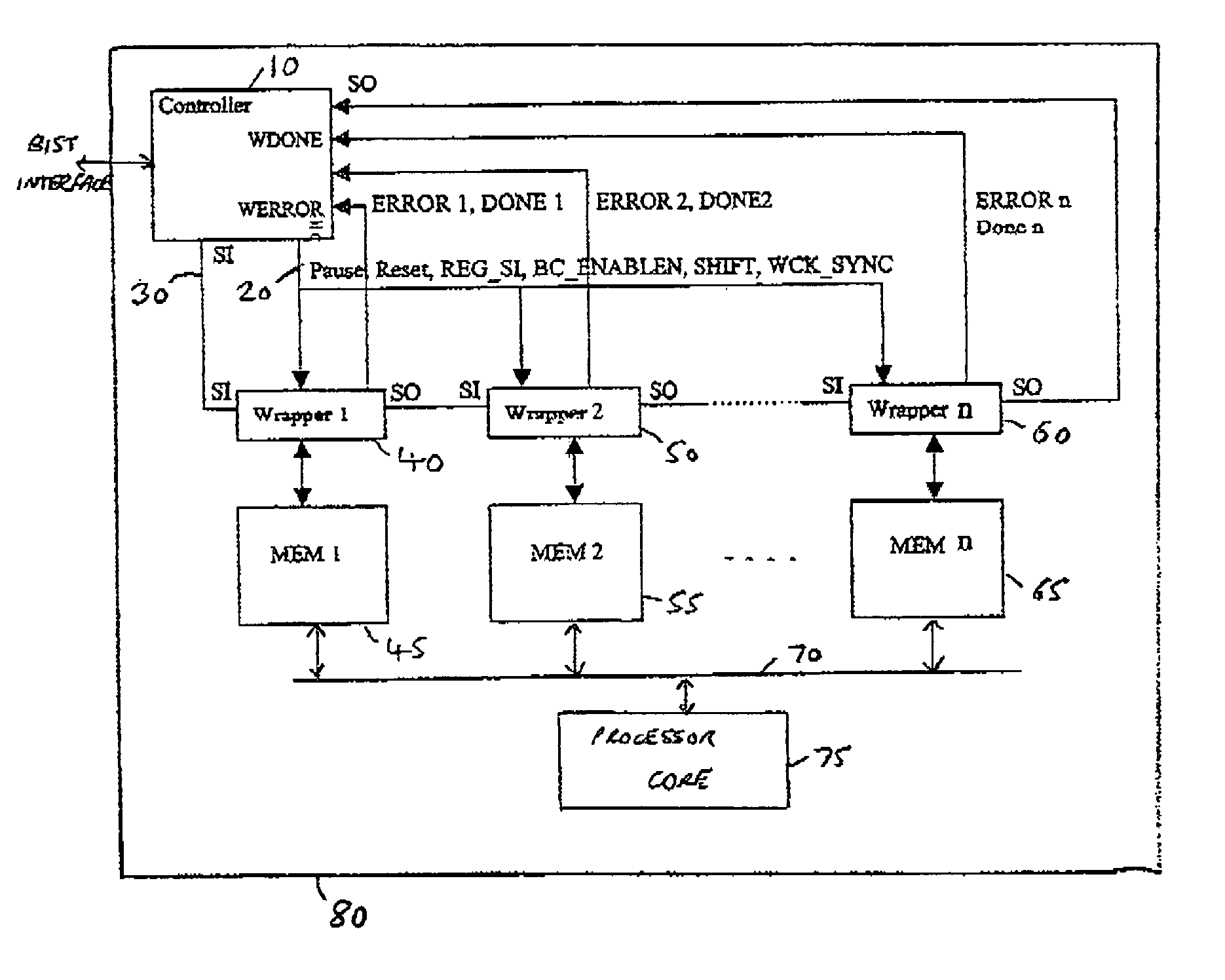
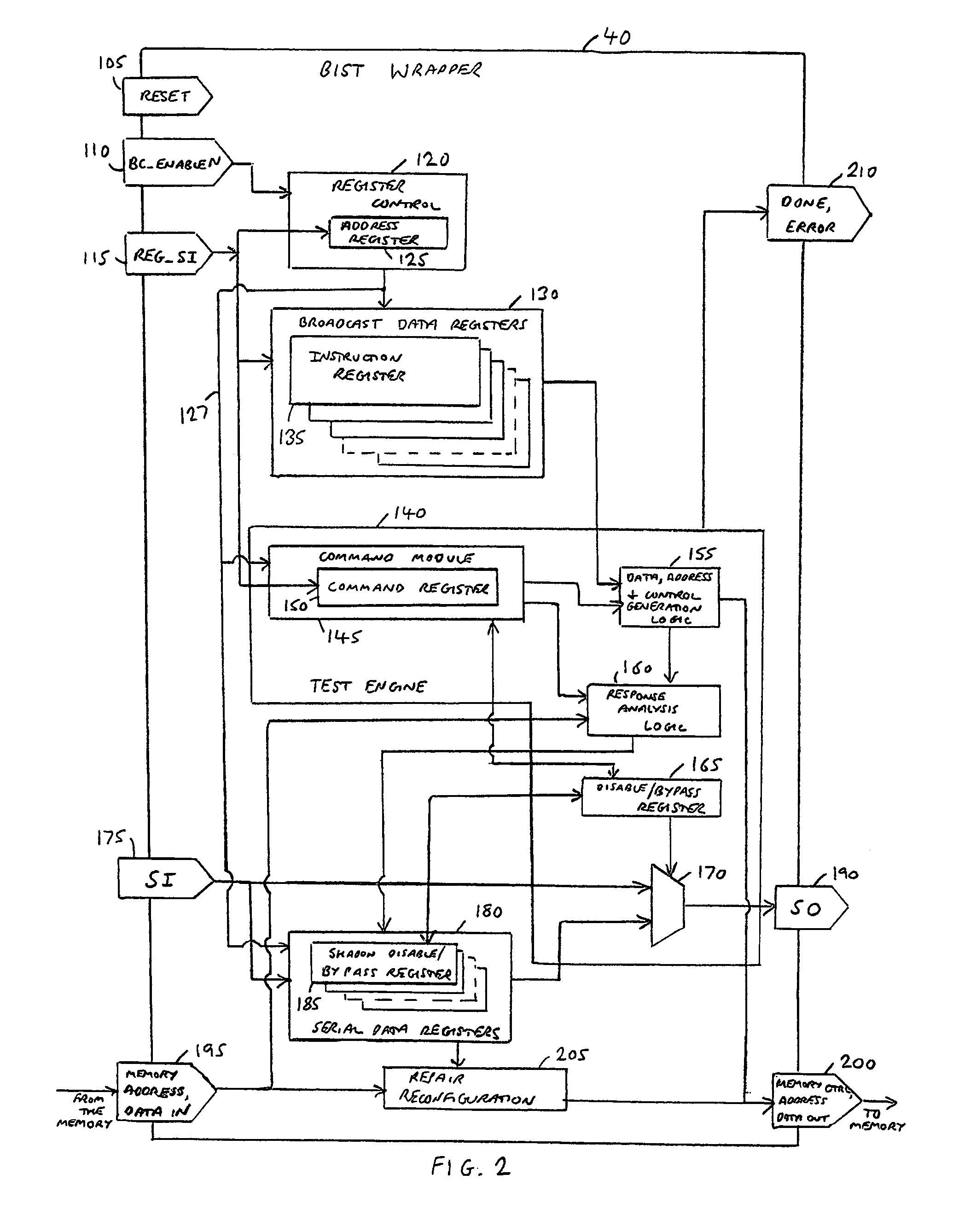
[0095]The Start Address Register is used in single step mode and is 8 bits in length, corresponding to an address space between 129 and 256 words in this embodiment. An address loaded into this register is used as the starting point for a single step instruction, unless it exceeds the address space of the memory, in which case no instruction is executed when the single step command is given.

[0096]The Write Mask Register is a 5-bit register determining which bits will be written during write enable test mode. When there are fewer write enable bits to the memory than bits in this register, only the least significant bits are used. When no write mask is present on the memory, a write enable test received by the wrapper will cause it to set its DONE bit to 1, and await further instructions.

[0097]Regarding the serial data registers 180, then as mentioned earlier, the scan c...


PUM


Abstract

An integrated circuit and method for testing memory on the integrated circuit are provided. The integrated circuit has processing logic for performing data processing operations on data, and a plurality of memory units for storing data for access by the processing logic. Further, memory test logic is provided to perform a sequence of tests in order to seek to detect memory defects in the memory units. The memory test logic comprises a plurality of test wrapper units, each test wrapper unit associated with one of the memory units and being operable to execute tests on the associated memory unit, and a test controller for controlling performance of the sequence of tests by communicating with each of the test wrapper units to provide test data defining each test to be executed by that test wrapper unit. Further, a first communication link is provided for connecting each of the test wrapper units directly to the test controller, and a second communication link is provided for connecting each test wrapper unit in an ordered sequence with the test controller. When controlling performance of the sequence of tests, the test controller provides first test data via the first communication link and second test data via the second communication link. It has been found that such an approach provides a particularly efficient and flexible technique for performing BIST functions within the integrated circuit.

Description

BACKGROUND OF THE INVENTION[0001]1. Field of the Invention[0002]The present invention relates to an integrated circuit and method for testing memory on the integrated circuit.[0003]2. Description of the Prior Art[0004]It is becoming more and more common for integrated circuits to include embedded memory to allow rapid access to data by processing logic provided on the integrated circuit. As the use of embedded memory continues to increase, thorough testing and defect diagnosis has become a key requirement to ensure product quality and enhance product yield. Whilst embedded memory presents significant system performance and cost reduction advantages, it brings its own testing issues. Externally generated test vector style tests are not suitable for verifying embedded memory arrays for a number of reasons. Firstly, the time spent in the manufacturing test grows exponentially as the embedded memory die area increases, which often makes such test vector style testing too costly. Further...

Claims


Application Information

Patent Timeline
Patent Type & Authority Patents(United States)
IPC IPC(8): G11C29/00G01R31/28
CPCG11C29/16
Inventor AITKEN, ROBERT CAMPBELLWAGGONER, GARY ROBERT
Owner ARM LTD
Why Eureka
Try Eureka