Semiconductor device
a technology a vf, applied in the direction of semiconductor devices, diodes, electrical devices, etc., can solve the problems of a large forward loss, long recovery time, and low switching characteristic, and achieve the effect of reducing the loss caused by a vf of a body diod
- Summary
- Abstract
- Description
- Claims
- Application Information
AI Technical Summary
Benefits of technology
Problems solved by technology
Method used
Image
Examples
first embodiment
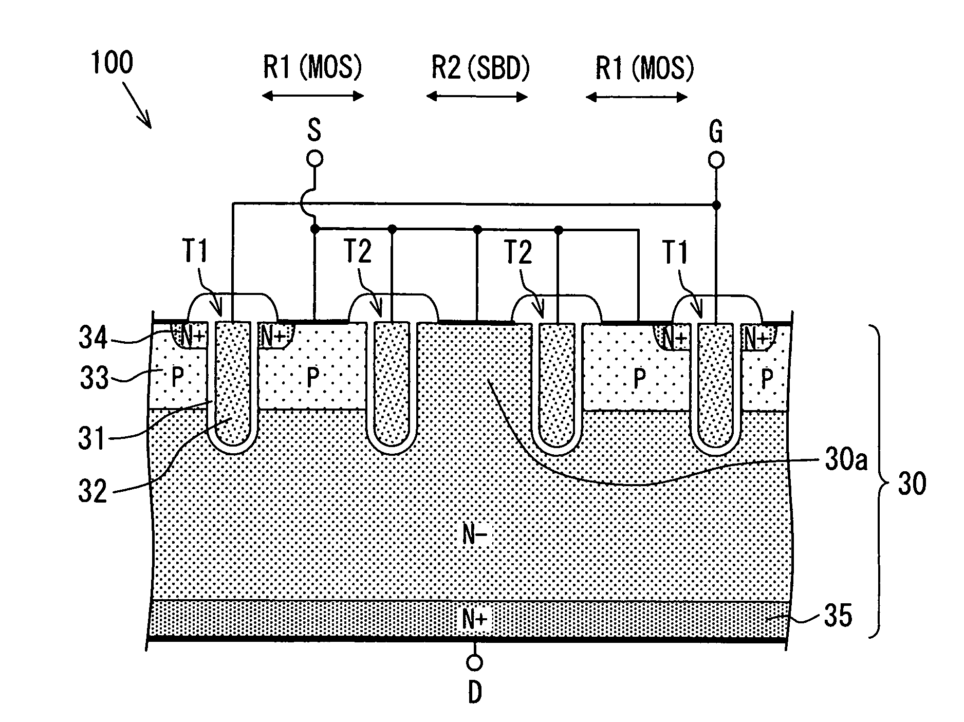
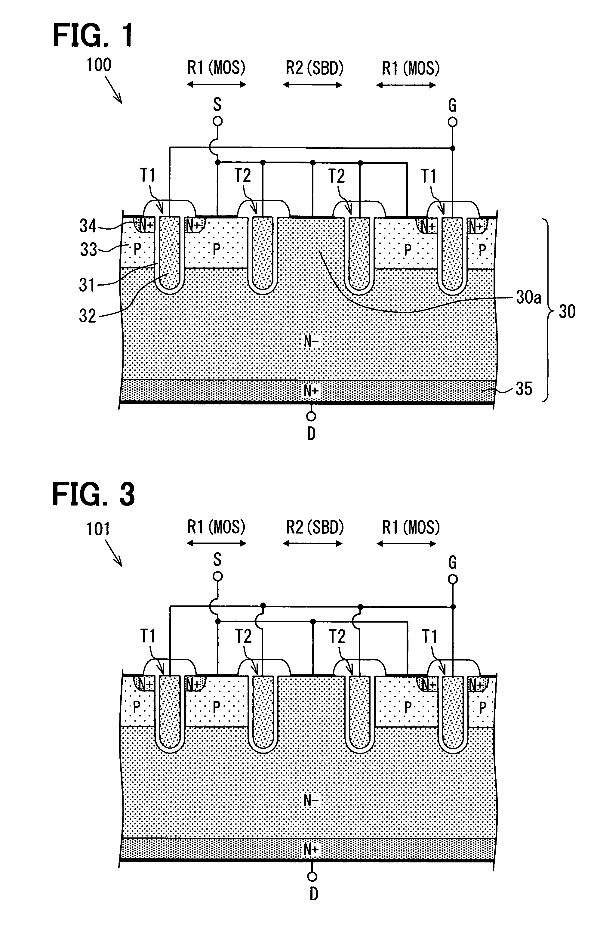
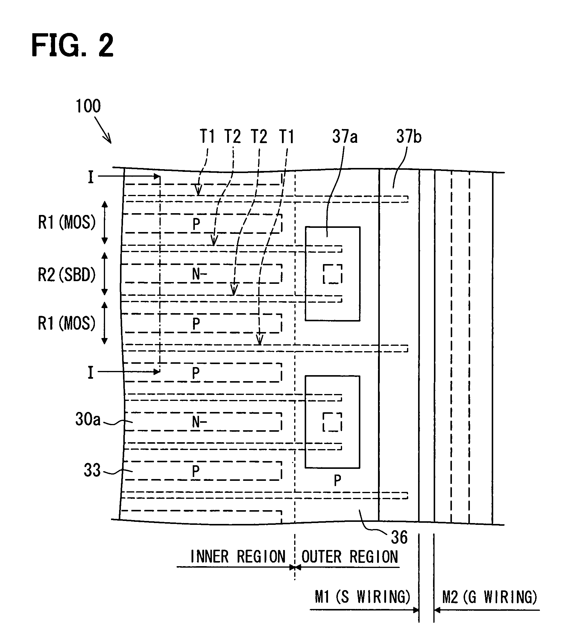
[0056]FIG. 1 shows an exemplary semiconductor device, that is, it is a schematic sectional view of a semiconductor device 100. FIG. 2 is a schematic plan view showing an exemplary planar pattern of an important part of the semiconductor device 100 of FIG. 1, and a sectional view taken along a chain line I-I in FIG. 2 corresponds to FIG. 1.
[0057]The semiconductor device 100 shown in FIGS. 1 and 2 is a semiconductor device in which a vertical MOS transistor (hereinafter abbreviated as MOS) having a trench gate structure and a Schottky barrier diode (hereinafter abbreviated as SBD) are formed adjacent to each other on an n-type (n−) semiconductor substrate 30. Although in the following example the vertical MOS transistor is an NMOSFET (n-channel metal oxide semiconductor field-effect transistor), it may be an IGBT (insulated-gate bipolar transistor) in which a p-type layer is provided on the back-surface side of the semiconductor substrate 30.
[0058]In the semiconductor device 100, as s...
second embodiment
[0092]A second embodiment will be hereinafter described. FIG. 19 shows a sectional structure of a semiconductor device according to this embodiment which is equipped with a DMOS having a trench gate structure. FIG. 20A is a schematic sectional view showing a wiring form of the semiconductor device of FIG. 19, and FIG. 20B shows its exemplary planar pattern. The configuration of the semiconductor device according to the embodiment will be described below with reference to FIG. 19 and FIGS. 20A and 20B.
[0093]The semiconductor device according to the embodiment is configured in such a manner that a DMOS having a trench gate structure and an AccuFET are formed adjacent to each other in a single chip. The AccuFET is a field-effect transistor which operates in an accumulation mode, that is, a MOSFET which is used for controlling a current flowing between trench by adjusting the widths of depletion layers formed between the trenches (refer to U.S. Pat. No. 4,903,189, for example).
[0094]As ...
third embodiment
[0115]FIG. 24 shows a sectional structure of a semiconductor device according to this embodiment which is equipped with a DMOS having a trench gate structure. FIG. 25A is a schematic sectional view showing a wiring form of the semiconductor device of FIG. 24, and 25B shows its exemplary planar pattern. The semiconductor device according to this embodiment is different from that according to the second embodiment only in that a J-FET is provided in place of the AccuFET. Therefore, only features that are different than in the second embodiment will be described.
[0116]The semiconductor device according to the embodiment is configured in such a manner that a DMOS having a trench gate structure and a J-FET are formed adjacent to each other in a single chip.
[0117]As shown in FIG. 24, second trenches 206c are formed in a J-FET forming region by digging the drift layer 202 from its surface. A p-type layer 213 is formed in a portion having a prescribed width around the inner wall surface of ...
PUM
 Abstract
Description
Claims
Application Information


