Semiconductor device

a technology a vf, applied in the direction of semiconductor devices, diodes, electrical devices, etc., can solve the problems of a large forward loss, long recovery time, and low switching characteristic, and achieve the effect of reducing the loss caused by a vf of a body diod

Active Publication Date: 2008-01-17
DENSO CORP
View PDF21 Cites 53 Cited by
  • Summary
  • Abstract
  • Description
  • Claims
  • Application Information

AI Technical Summary

Benefits of technology

[0019] In the device, the MOS transistor and the Schottky barrier diode are reversely coupled with each other. Accordingly, the device can provide a switching element in an inverter circuit. In this case, the Schottky barrier diode has a low threshold voltage, compared with a PN junction diode. Thus, a recovery property and a forward direction loss in the Schottky barrier diode are improved.
[0020] Further, since the MOS transistor and the Schottky barrier diode are proximately arranged, so that a switching property is improved, and further, dimensions and a manufacturing cost of the device are reduced. Furthermore, by designing a width between two trenches appropriately, a withstand voltage of the MOS transistor is improved. Further, since the second conductive type layer for providing the channel region of the MOS transistor is limited to diffuse in a lateral direction of the substrate by the trench, impurity concentration is easily controlled, and a parasitic operation of a parasitic bipolar transistor is reduced so that a load surge breakdown voltage is improved.
[0021] Thus, the recovery property and the forward direction loss are improved, and the withstand voltage and the surge breakdown voltage in the transistor are also improved. Thus, the switching property in the device is improved, and the dimensions of the device are small.
[0023] In the above device, a return current flows through the accumulation FET instead of the MOSFET. Thus, loss caused by a Vf of a body diode is reduced.
[0025] In the above device, a return current flows through the J-FET instead of the MOSFET. Thus, loss caused by a Vf of a body diode is reduced.

Problems solved by technology

However, the body diode which is formed in the above manner has problems of a long recovery time and a large forward loss.
Therefore, the semiconductor device 90 has problems that the switching characteristic is basically bad and the chip cost is high because of an increased chip area.
However, this configuration raises another problem that the increased intervals between the gate trenches lower the breakdown voltage of the MOS.
This means a problem that the L load surge resistance is low.
Where the semiconductor devices having the above structure are applied to an H-bridge circuit such as a motor drive circuit and the individual MOSFETs are on / off-driven by a PWM control, a return current flows through the body diodes of the MOSFETs located on the high side, which causes a return current loss which is mainly due to Vf of the body diodes.

Method used


Image

  • Semiconductor device
  • Semiconductor device
  • Semiconductor device

Examples


first embodiment

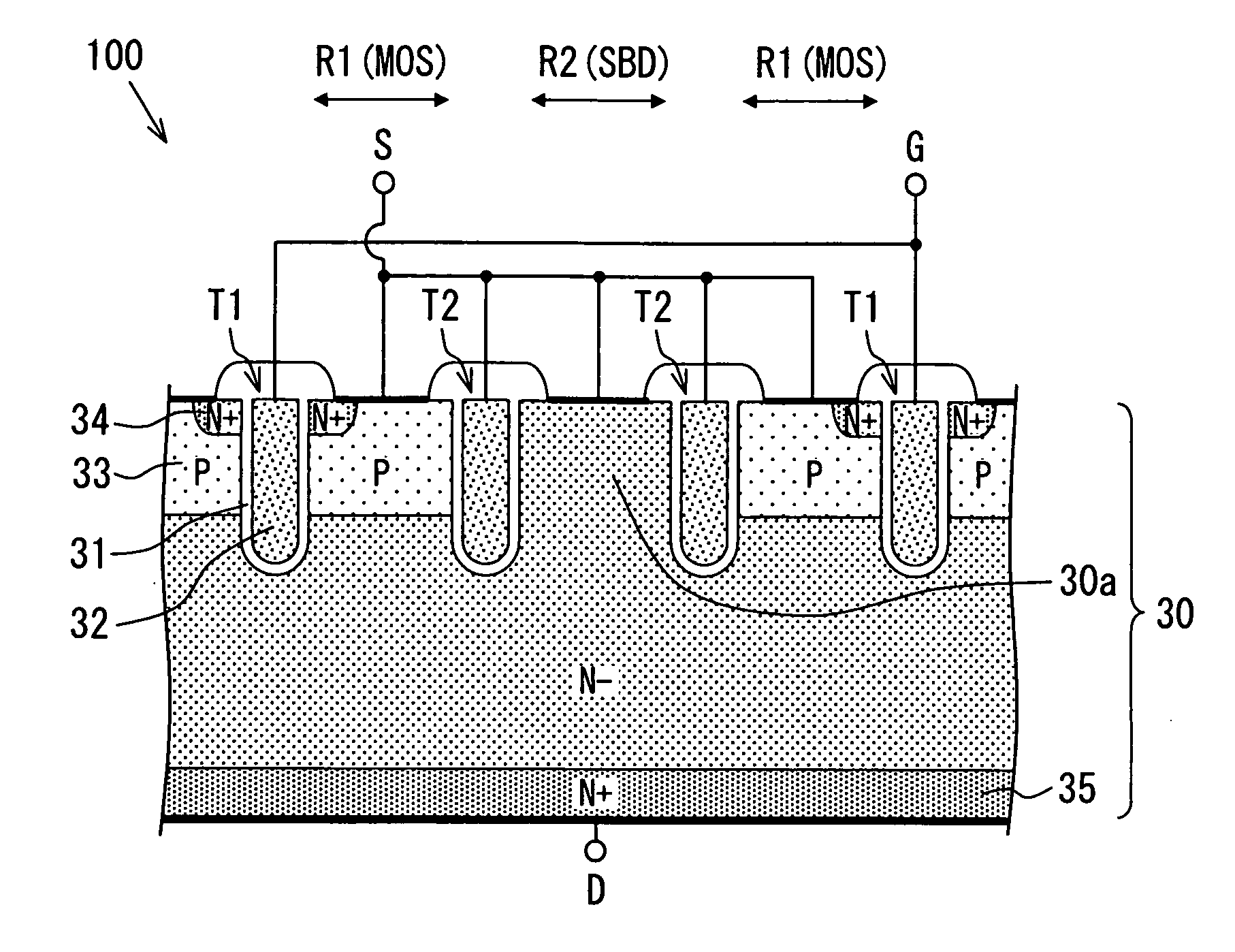
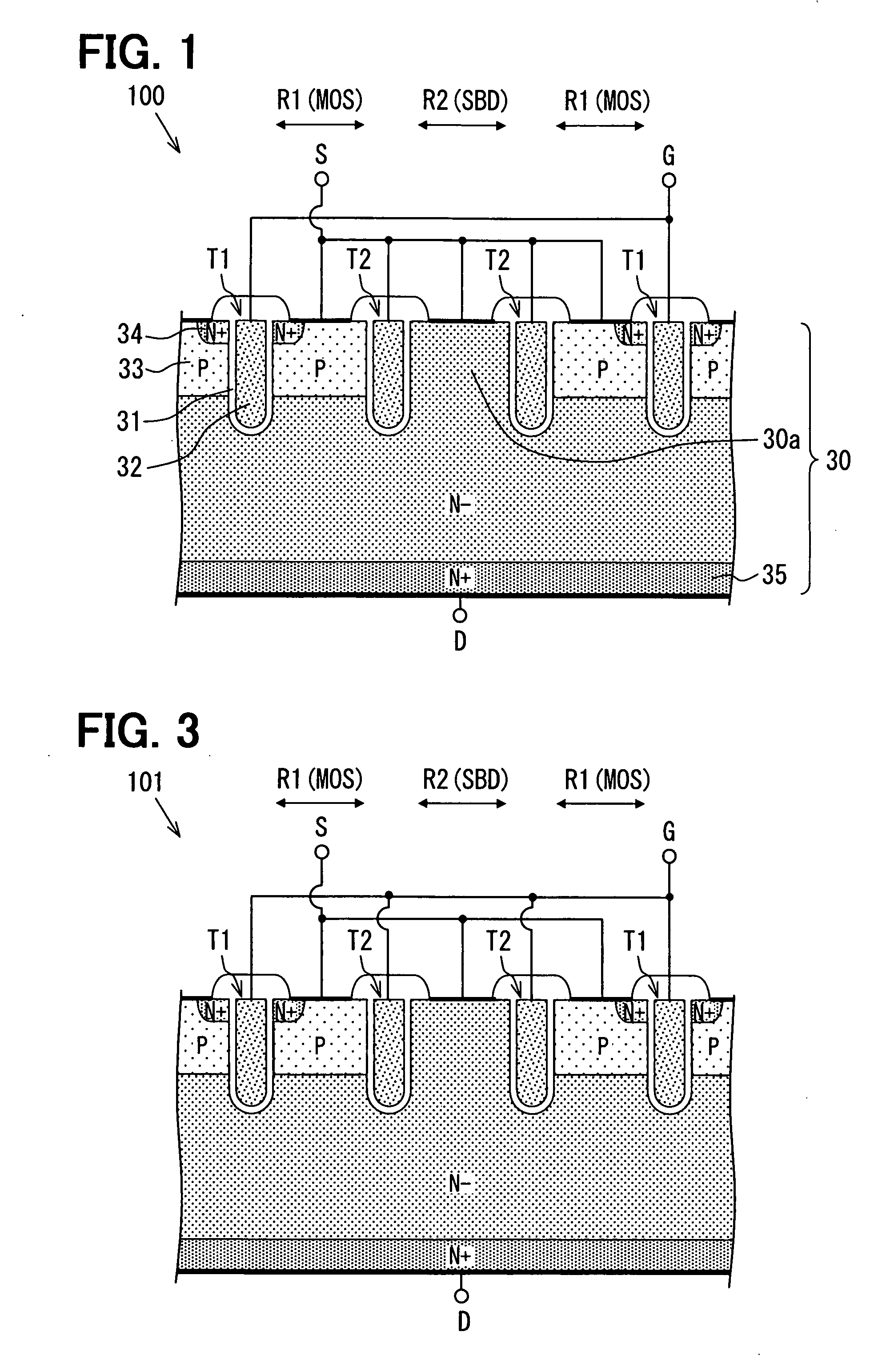
[0056]FIG. 1 shows an exemplary semiconductor device, that is, it is a schematic sectional view of a semiconductor device 100. FIG. 2 is a schematic plan view showing an exemplary planar pattern of an important part of the semiconductor device 100 of FIG. 1, and a sectional view taken along a chain line I-I in FIG. 2 corresponds to FIG. 1.

[0057] The semiconductor device 100 shown in FIGS. 1 and 2 is a semiconductor device in which a vertical MOS transistor (hereinafter abbreviated as MOS) having a trench gate structure and a Schottky barrier diode (hereinafter abbreviated as SBD) are formed adjacent to each other on an n-type (n−) semiconductor substrate 30. Although in the following example the vertical MOS transistor is an NMOSFET (n-channel metal oxide semiconductor field-effect transistor), it may be an IGBT (insulated-gate bipolar transistor) in which a p-type layer is provided on the back-surface side of the semiconductor substrate 30.

[0058] In the semiconductor device 100, ...

second embodiment

[0092] A second embodiment will be hereinafter described. FIG. 19 shows a sectional structure of a semiconductor device according to this embodiment which is equipped with a DMOS having a trench gate structure. FIG. 20A is a schematic sectional view showing a wiring form of the semiconductor device of FIG. 19, and FIG. 20B shows its exemplary planar pattern. The configuration of the semiconductor device according to the embodiment will be described below with reference to FIG. 19 and FIGS. 20A and 20B.

[0093] The semiconductor device according to the embodiment is configured in such a manner that a DMOS having a trench gate structure and an AccuFET are formed adjacent to each other in a single chip. The AccuFET is a field-effect transistor which operates in an accumulation mode, that is, a MOSFET which is used for controlling a current flowing between trench by adjusting the widths of depletion layers formed between the trenches (refer to U.S. Pat. No. 4,903,189, for example).

[0094...

third embodiment

[0115]FIG. 24 shows a sectional structure of a semiconductor device according to this embodiment which is equipped with a DMOS having a trench gate structure. FIG. 25A is a schematic sectional view showing a wiring form of the semiconductor device of FIG. 24, and 25B shows its exemplary planar pattern. The semiconductor device according to this embodiment is different from that according to the second embodiment only in that a J-FET is provided in place of the AccuFET. Therefore, only features that are different than in the second embodiment will be described.

[0116] The semiconductor device according to the embodiment is configured in such a manner that a DMOS having a trench gate structure and a J-FET are formed adjacent to each other in a single chip.

[0117] As shown in FIG. 24, second trenches 206c are formed in a J-FET forming region by digging the drift layer 202 from its surface. A p-type layer 213 is formed in a portion having a prescribed width around the inner wall surface...


PUM


Abstract

A semiconductor device includes: a semiconductor substrate; a vertical type trench gate MOS transistor; a Schottky barrier diode; multiple trenches having a stripe pattern to divide an inner region into first and second separation regions; and a poly silicon film in each trench. The first separation region includes a first conductive type region for providing a source and a second conductive type layer for providing a channel region. The first conductive type region is adjacent to a first trench. The poly silicon film in the first trench is coupled with a gate wiring. A second trench is not adjacent to the first conductive type region. The poly silicon film in the second trench is coupled with a source or gate wiring. The substrate in the second separation region is coupled with the source wiring for providing a Schottky barrier.

Description

CROSS REFERENCE TO RELATED APPLICATIONS [0001] This application is based on Japanese Patent Applications No. 2006-194527 filed on Jul. 14, 2006, and No. 2007-115581 filed on Apr. 25, 2007, the disclosures of which are incorporated herein by reference. FIELD OF THE INVENTION [0002] The present invention relates to a semiconductor device. BACKGROUND OF THE INVENTION [0003] Inverter circuits for driving a load such as a motor for use in a vehicle are DC to AC converters; that is, they convert a DC voltage to an AC voltage and supply the latter to a load such as a motor. An inverter circuit for driving a motor which is inductive is composed of a MOS transistor (hereinafter abbreviated as MOS) or an insulated-gate bipolar transistor (hereinafter abbreviated as IGBT) as a switching element and a free-wheel diode (hereinafter abbreviated as FWD). The FWD bypasses and returns a current that flows through the motor while the MOS is off so that the current flowing through the motor is not var...

Claims


Application Information

Patent Timeline
Patent Type & Authority Applications(United States)
IPC IPC(8): H01L29/80H01L29/76
CPCH01L29/0696H01L29/4236H01L29/42368H01L29/66666H01L29/8083H01L29/7803H01L29/7806H01L29/7813H01L29/7828H01L29/66734H01L29/7811
Inventor AOKI, TAKAAKIFUJII, TETSUOSHIGA, TOMOFUSA
Owner DENSO CORP
Why Eureka
Try Eureka