Multilayer ceramic electronic component including external electrodes that include a plating layer having a low film stress

a multi-layer ceramic and external electrode technology, applied in the direction of fixed capacitors, stacked capacitors, fixed capacitor details, etc., can solve the problems of difficult reduction of compressive stress, disadvantageous swelling of the surface of the plating layer, etc., and achieve low film stress, high effective volume fraction, and superior appearance

Active Publication Date: 2012-04-10
MURATA MFG CO LTD
View PDF24 Cites 5 Cited by
  • Summary
  • Abstract
  • Description
  • Claims
  • Application Information

AI Technical Summary

Benefits of technology

[0015]To overcome the problems described above, preferred embodiments of the present invention provide a multilayer ceramic electronic component including external electrodes, each including at least one plating layer having a very low film stress and having a high effective volume fraction, superior appearance, and superior reliability.
[0020]Since the external electrode is substantially made of at least one plating layer, the ceramic electronic component has a superior effective volume fraction. When the film stress of the plating layer is compressive, the compressive film stress is about 100 MPa or less. Consequently, the swelling at the surface of the plating layer, which is difficult to prevent in the known external layer, can be effectively prevented. When the film stress of the plating layer is tensile, the tensile film stress is about 100 MPa or less. Consequently, a connection failure with the internal electrodes, which is difficult to prevent in the known external layer, can be effectively prevented.

Problems solved by technology

It has however been discovered that when a plating layer is directly formed on the surface of the ceramic stack at which the internal electrodes are exposed, without disposing a paste electrode layer between the surface of the ceramic stack and the plating layer, as disclosed in Japanese Unexamined Patent Application Publication No. 63-169014, the film stress of the plating layer as disclosed in Japanese Unexamined Patent Application Publication No. 2002-170733, that is, 490 MPa, is not sufficient and may result in problems.
More specifically, when the film stress of the plating layer is compressive, that is, when the plating layer tends to extend in the horizontal direction, many swellings disadvantageously occur at the surface of the plating layer.
This is likely due to the fact that the plating layer is formed on a significantly uneven surface at which ceramic and the internal electrodes are present together, and consequently, the compressive stress is difficult to reduce.

Method used


Image

  • Multilayer ceramic electronic component including external electrodes that include a plating layer having a low film stress
  • Multilayer ceramic electronic component including external electrodes that include a plating layer having a low film stress
  • Multilayer ceramic electronic component including external electrodes that include a plating layer having a low film stress

Examples


Embodiment Construction

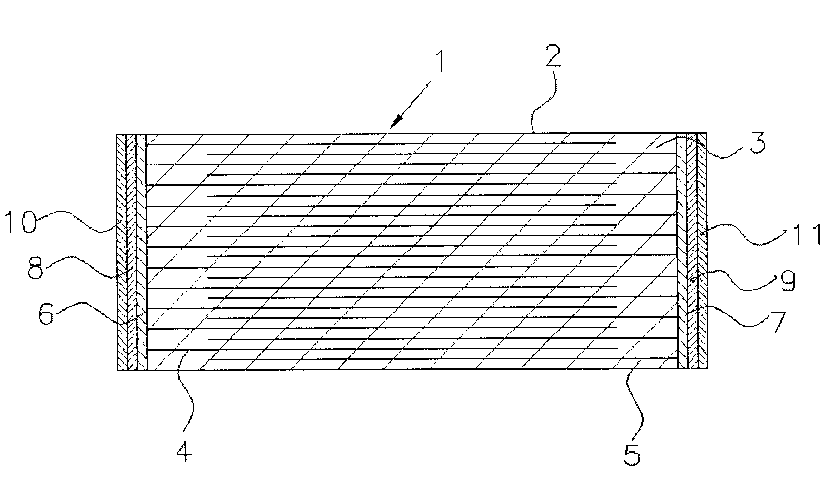
[0026]In various preferred embodiments of the present invention, the external electrode includes a plating layer directly formed on the surface at which the internal electrodes are exposed without forming a paste electrode layer, a sputter electrode layer, a vapor-deposited electrode layer, or any other suitable interlayer of the external electrode. FIG. 1 shows a multilayer ceramic capacitor, which is a type of multilayer ceramic electronic component, according to a preferred embodiment of the present invention.

[0027]The multilayer ceramic capacitor 1 shown in FIG. 1 includes a laminate 2 including a stack of a plurality of dielectric ceramic layers 3 and a plurality of internal electrodes 4 and 5 extending along interfaces between the dielectric ceramic layers, and external electrodes electrically connecting the internal electrodes 4 or 5 exposed at the respective surfaces of the laminate 2. To form the external electrodes, first, first plating layers 6 and 7 are formed on the res...


PUM

PropertyMeasurementUnit
compressiveaaaaaaaaaa
thermal stressaaaaaaaaaa

Abstract

A multilayer ceramic electronic component includes a laminate including a stack of a plurality of ceramic layers and a plurality of internal electrodes extending along interfaces between the ceramic layers, and a plurality of external electrodes electrically connecting the internal electrodes exposed at surfaces of the laminate. Each external electrode includes a plating layer at least at the portion directly connected to the internal electrodes. The plating layer has a compressive film stress of about 100 MPa or less or a tensile film stress of about 100 MPa or less.

Description

BACKGROUND OF THE INVENTION[0001]1. Field of the Invention[0002]The present invention relates to a multilayer ceramic electronic component, and more particularly to an external electrode of the multilayer ceramic electronic component.[0003]2. Description of the Related Art[0004]A multilayer ceramic capacitor, which is a known multilayer ceramic electronic component, includes a laminate including a stack of a plurality of dielectric ceramic layers and a plurality of internal electrodes extending along interfaces between the dielectric ceramic layers, and a plurality of external electrodes each electrically connecting the internal electrodes exposed at a surface of the laminate. Such a known multilayer ceramic capacitor is shown in FIG. 4.[0005]According to FIG. 4, the external electrodes are respectively formed on the surfaces of the laminate 102 at which the internal electrodes 104 and 105 are exposed, and thus are electrically connecting the internal electrodes 104 or 105. In order...

Claims


Application Information

Patent Timeline
Patent Type & Authority Patents(United States)
IPC IPC(8): H01G4/228H01G4/06
CPCH01G4/005H01G4/008H01G4/12H01G4/30
Inventor MOTOKI, AKIHIROOGAWA, MAKOTOTAKEUCHI, SHUNSUKEKAWASAKI, KENICHI
Owner MURATA MFG CO LTD
Why Eureka
Try Eureka