
Method of forming an electroded sheet

a technology of electroded sheets and electrodes, applied in the field of electroded sheets, can solve the problems of limiting the size of display types, affecting the conductive pattern formation of cell components, and creating the top column electrode plates, and achieve good electrical connection and high conductivity

Inactive Publication Date: 2012-05-01
MOORE CHAD B
View PDF87 Cites 41 Cited by
  • Summary
  • Abstract
  • Description
  • Claims
  • Application Information

AI Technical Summary

Benefits of technology

Enables high-speed addressing of large displays with reduced resistance and cost, allowing for uniform voltage application along the electrode lines, thereby improving the speed and efficiency of addressing electro-optic materials.

Problems solved by technology

However, this passive addressing scheme requires that the electro-optic material has a threshold or its optical properties have an abrupt change over a small change in applied voltage.
Some of the liquid crystal materials use an active transistor back plane to address the displays, but these types of displays are presently limited in size due to a complicated and costly manufacturing process.
Transmissive displays using liquid crystal materials and a plasma-addressed back plane have been demonstrated in U.S. Pat. No. 4,896,149, herein incorporated by reference, however, these plasma-addressed back planes are also limited in size due to availability of the thin microsheet to create the plasma cells.
One potential issue in producing large plasma-addressed tubular displays is creating the top column electrode plate.
A traditional patterned indium tin oxide (ITO) transparent conductor works fine for smaller panels where processing the panel is easy and the lines are short, however to address very large panels, the ITO lines are not conductive enough and patterning of the lines becomes very expensive.

Method used


Image

  • Method of forming an electroded sheet
  • Method of forming an electroded sheet
  • Method of forming an electroded sheet

Examples


example

[0204]This example uses an aluminum drum, 9″OD×6.5″L×¼″ walls (28.3″ circumference). A piece of polymer coated PET (MacTac TL5100 10 Mil Matte Polyester-7 mil thick Mylar® film with 3 mil thick polymeric adhesive) is cut 6″ wide by 25″ long. Double stick tape is used to attach both ends of the TL5100 film to the drum, polymer film facing outward. Once the TL5100 film is in place, 0.003″D Kovar wire is wrapped around the drum over the TL5100 film on a 0.100″ pitch. Next the drum is placed in an oven at 130° C. for ½ hour. Calculations show that the 9″D aluminum drum expands 0.0228″ in diameter going from 20° C. to 130° C., and the Kovar wire wrap diameter expands 0.0059″. This difference of 0.0169″ easily pushes the wires into the 0.003″ polymer coating. Once the drum is at 130° C. and the wire is sunk into the polymer film, the Kovar wire is stretched 0.0343″ for each turn on the drum resulting in a total stress on the wire electrode of 24,200 psi. Since the yield stress of Kovar is...


PUM

PropertyMeasurementUnit
thickaaaaaaaaaa
thickaaaaaaaaaa
transparentaaaaaaaaaa

Abstract

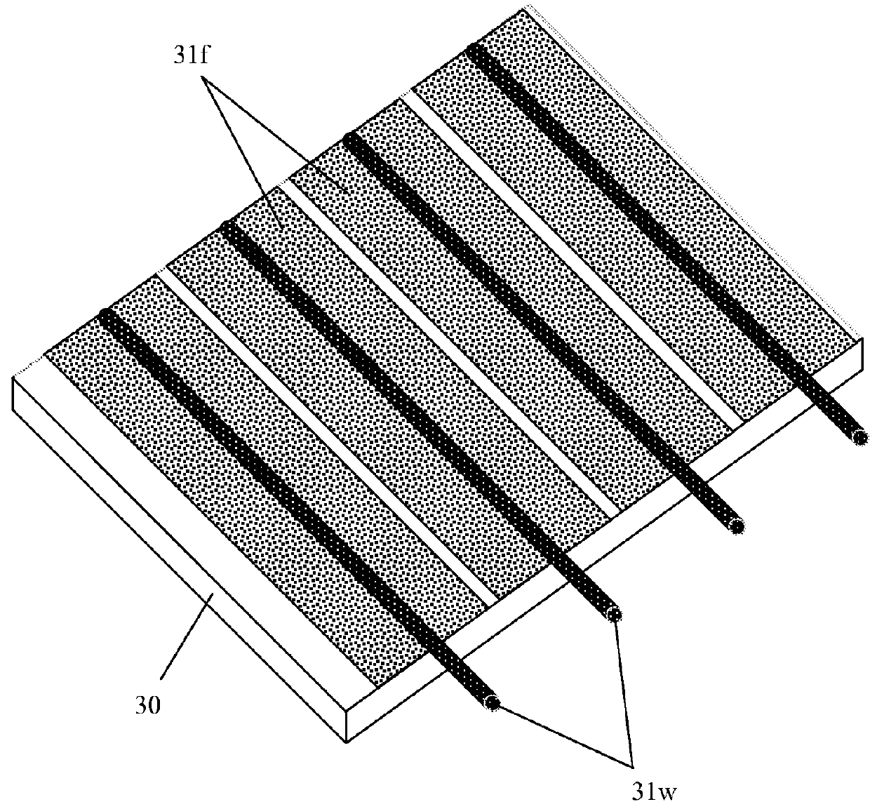
A sheet in an electronic display is composed of a substrate containing an array of wire electrodes. The wire electrodes are preferably electrically connected to patterned transparent conductive electrode lines. The wire electrodes are used to carry the bulk of the current. The wire electrodes are capable of being extended away from the substrate and connected directly to the printed circuit board. The transparent conductive electrode (TCE) is used to spread the charge or voltage from the wire electrode across the pixel. The TCE is a patterned film and must be at least 50% transparent, and, for most applications, is preferably over 90% transparent. In most applications, the electroded surface of the electroded sheet has to be flattened. Use of a thin polymer substrate yields a light, flexible, rugged sheet that may be curved, bent or rolled.

Description

REFERENCE TO RELATED APPLICATIONS[0001]This application claims one or more inventions which were disclosed in Provisional Application No. 60 / 957,317, filed Aug. 22, 2007, entitled “ELECTRODED SHEET” and Provisional Application No. 61 / 060,614, filed Jun. 11, 2008, entitled “ELECTRODED SHEET (eSHEET) PRODUCTS”. The benefit under 35 USC §119(e) of the United States provisional applications is hereby claimed, and the aforementioned applications are hereby incorporated herein by reference.[0002]This application is also a continuation in part of copending U.S. application Ser. No. 11 / 609,093, filed Dec. 11, 2006, entitled “TUBULAR PLASMA DISPLAY”, copending U.S. application Ser. No. 11 / 609,131, filed Dec. 11, 2006, entitled “ELECTRODED SHEET”, copending U.S. application Ser. No. 11 / 609,220, filed Dec. 11, 2006, entitled “WIRE-BASED FLAT PANEL DISPLAYS”, and copending PCT Patent Application Number PCT / US2006 / 061872, filed Dec. 11, 2006, entitled “WIRE-BASED FLAT PANEL DISPLAYS, which all c...

Claims


Application Information

Patent Timeline
Patent Type & Authority Patents(United States)
IPC IPC(8): H01K3/10H05K1/03
CPCG06F3/0412G06F3/045H01J17/04H01L31/02008H01L31/022425H01M4/02H01M4/8605H01L31/0516G06F3/044Y10T29/49162H01L51/445Y02E10/50Y02E60/50Y10T29/49165Y10T29/49126Y10T29/49155Y10T29/4913Y10T29/49128G06F3/0445G06F3/0446H10K30/83
Inventor MOORE, CHAD B.
Owner MOORE CHAD B
Learn More