
Fusion memory device embodied with phase change memory devices having different resistance distributions and data processing system using the same

a phase change memory and fusion memory technology, applied in semiconductor devices, digital storage, instruments, etc., can solve the problems the operating speed of flash memory is often relatively slow, and achieve the effect of increasing the capacitor capacity

Active Publication Date: 2012-05-08
SK HYNIX INC
View PDF9 Cites 5 Cited by
  • Summary
  • Abstract
  • Description
  • Claims
  • Application Information

AI Technical Summary

Benefits of technology

The patent describes a fusion memory device that includes two groups of phase change memory cells. The first group has a different resistance distribution compared to the second group during phase-changing. The first group can replace flash memory, while the second group can replace DRAM. The first group has a higher sensing ratio, while the second group has a lower sensing ratio. The first group has fully phase-changed cells, while the second group has partially phase-changed cells. The second group has smaller cells. The patent also describes a data processing system that includes a CPU, a data storage block, and a work memory block. The data storage block includes a first phase change memory group, while the work memory block includes a second phase change memory group. The second group has lower reset resistance than the first group.

Problems solved by technology

However, DRAMs require carrying out periodic refresh operations due to their volatile properties and require an increased capacitor capacity due to demand for high charge storage.
Furthermore, since it is difficult to randomly access, data is programmed at a page unit, and thereby operating speeds of flash memories are often relatively slow.

Method used


Image

  • Fusion memory device embodied with phase change memory devices having different resistance distributions and data processing system using the same
  • Fusion memory device embodied with phase change memory devices having different resistance distributions and data processing system using the same
  • Fusion memory device embodied with phase change memory devices having different resistance distributions and data processing system using the same

Examples


Embodiment Construction

.”

BRIEF DESCRIPTION OF THE DRAWINGS

[0019]The above and other aspects, features and other advantages of the subject matter of the present disclosure will be more clearly understood from the following detailed description taken in conjunction with the accompanying drawings, in which:

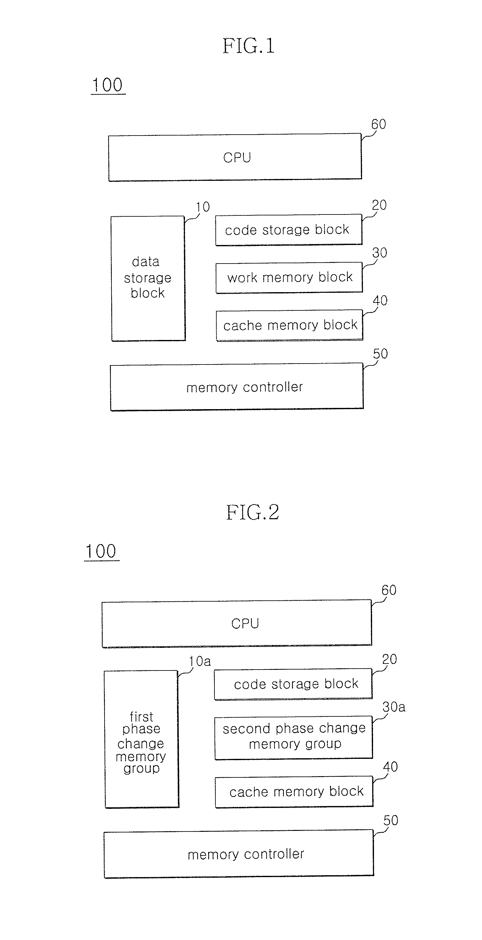
[0020]FIG. 1 is a block diagram illustrating a data processing system as an example of a fusion memory device according to the inventive concept;

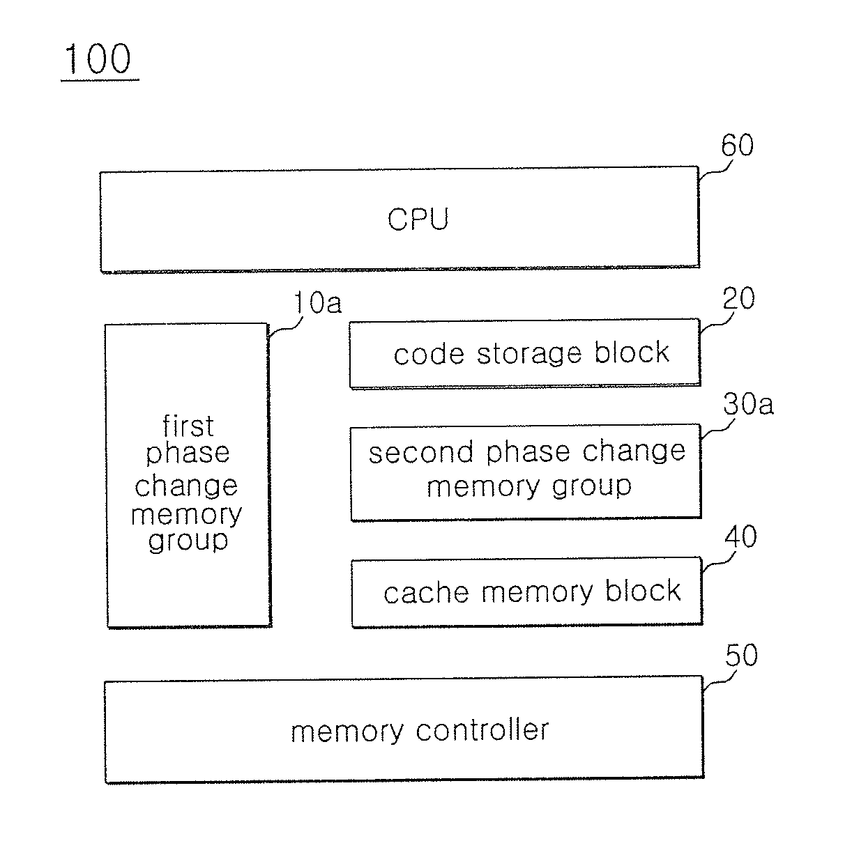
[0021]FIG. 2 is a block diagram illustrating a data processing system according to an example embodiment;

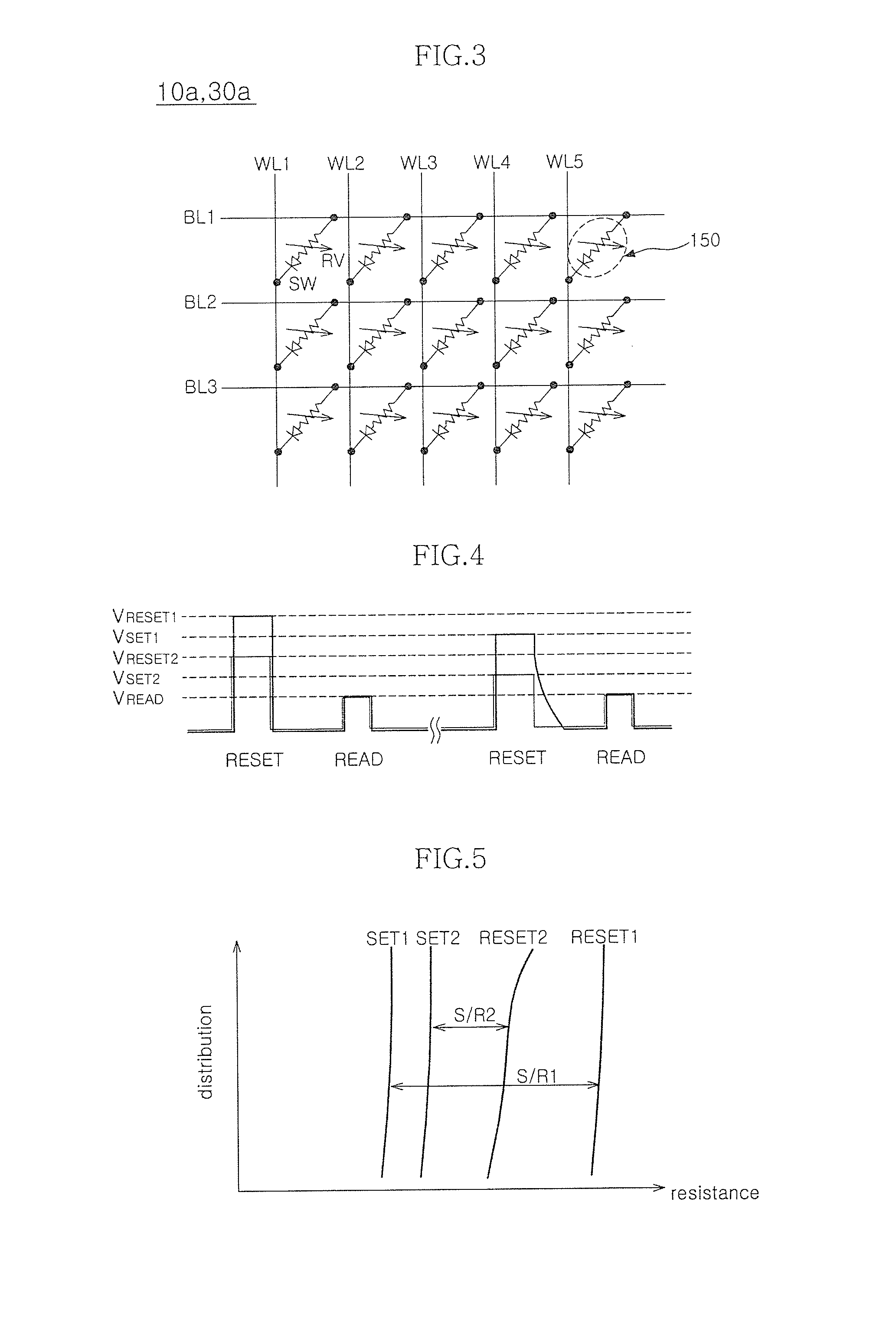
[0022]FIG. 3 is a schematic circuit diagram of first and second phase change memory groups according to the example embodiment;

[0023]FIG. 4 is a diagram showing voltage program conditions of the first and second phase change memory groups according to the example embodiment;

[0024]FIG. 5 is a graph showing resistance distributions of the first and second memory groups according to the example embodiment;

[0025]FIG. 6 is a plan view of a fusion memory device inclu...


PUM


Abstract

A fusion memory device having phase change memory devices that have different resistance distributions and a corresponding data processing system is presented. The fusion memory device includes a first and a second phase change memory group arranged on the same chip. Because the second phase change memory group exhibits a resistance distribution different from that of the first phase change memory group, then the fusion memory device can be configured to simultaneously function as both a DRAM device and as a flash memory device. Because the first and second phase change memory groups can be composed of similar PRAM components, the corresponding manufacturing and driving circuitry is markedly simplified as compared to other fusion memory devices that have dissimilar DRAM and flash memory components.

Description

CROSS-REFERENCES TO RELATED APPLICATION[0001]The present application claims priority under 35 U.S.C. 119(a) to Korean application numbers 10-2009-0054891 and 10-2009-0071244, filed on Jun. 19, 2009 and Aug. 3, 2009, respectively, in the Korean Patent Office, which are incorporated by reference in its entirety as if set forth in full.BACKGROUND OF THE INVENTION[0002]1. Technical Field[0003]The embodiments described herein relate to semiconductor integrated devices and, more particularly, to a fusion memory device composed of memory devices that exhibit different functions and a data processing system using the same.[0004]2. Related Art[0005]Memory device can be classified into a volatile memory devices and a non-volatile memory devices. The volatile memory devices include random access memories (RAM) which data stored therein are erased when the power is off. Non-volatile memory devices include read only memories (ROM) which data stored therein is retained when power is off. Typicall...

Claims


Application Information

Patent Timeline
Patent Type & Authority Patents(United States)
IPC IPC(8): G11C11/00
CPCG11C11/5678G11C13/0004G11C13/0033H01L27/2409H01L27/2463H01L45/06H01L45/1233H01L45/126G11C11/005G11C2213/72H10B63/20H10B63/80H10N70/8413H10N70/231H10N70/826
Inventor LEE, SE HO
Owner SK HYNIX INC
Learn More