Top feature package and method

a technology of electronic components and top features, applied in the field of electronic components, can solve the problems of increasing the overall cost of wireless electronic component packages and restricting the ability to miniaturize wireless electronic component packages, and achieve the effect of minimizing the overall package manufacturing cost and minimizing the overall package siz

Active Publication Date: 2012-06-12
AMKOR TECH SINGAPORE HLDG PTE LTD
View PDF32 Cites 100 Cited by
  • Summary
  • Abstract
  • Description
  • Claims
  • Application Information

AI Technical Summary

Benefits of technology

[0007]A package body encloses the electronic component, the package body having a principal surface. An antenna is formed on the principal surface by applying an electrically conductive coating. An embedded interconnect extends through the package body between the substrate and the principal surface and electrically connects the second antenna terminal to the antenna. Applying an electrically conductive coating to form the antenna is relatively simple thus minimizing the overall package manufacturing cost. Further, the antenna is relatively thin thus minimizing the overall package size.

Problems solved by technology

However, the antenna mounting requires special tooling and additional assembly operations thus increasing the overall cost of the wireless electronic component package.
Further, space must be allocated for the antenna thus restricting the ability to miniaturize the wireless electronic component package.

Method used


Image

  • Top feature package and method
  • Top feature package and method
  • Top feature package and method

Examples


Embodiment Construction

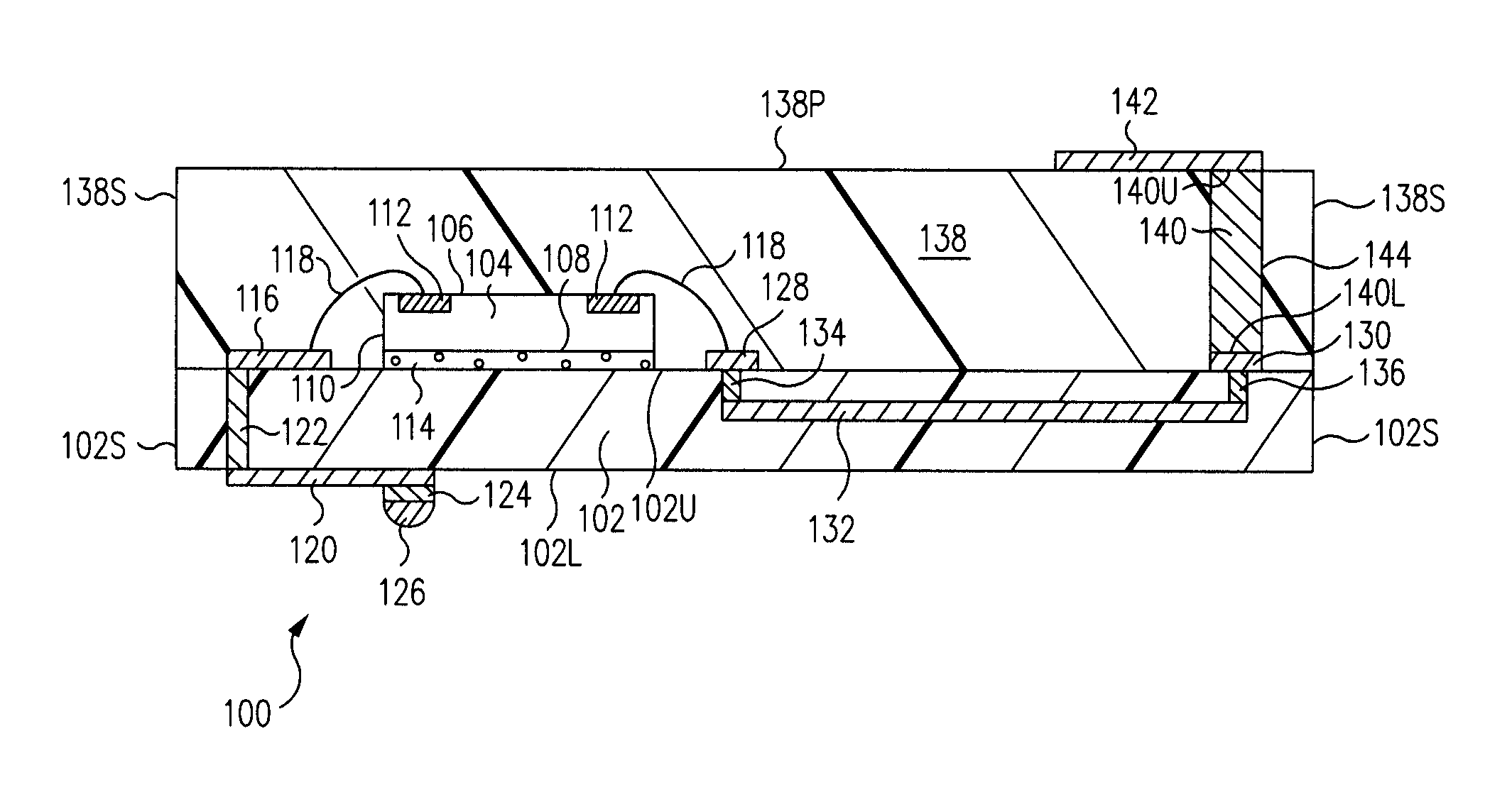
[0023]FIG. 1 is a cross-sectional view of a wireless electronic component package 100 in accordance with one embodiment. Wireless electronic component package 100, sometimes called an electronic component package, includes a substrate 102. Substrate 102 is a dielectric material such as laminate, ceramic, printed circuit board material, or other dielectric material.

[0024]Substrate 102 includes an upper, e.g., first, surface 102U and an opposite lower, e.g., second, surface 102L. Substrate 102 further includes sides 102S extending perpendicularly between upper surface 102U and lower surface 102L. Although the terms parallel, perpendicular, and similar terms are used herein, it is to be understood that the described features may not be exactly parallel and perpendicular, but only substantially parallel and perpendicular to within accepted manufacturing tolerances.

[0025]Wireless electronic component package 100 further includes an electronic component 104, e.g., a single die. In one emb...


PUM


Abstract

An electronic component package includes a substrate and an electronic component mounted to the substrate, the electronic component including a bond pad. A first antenna terminal is electrically connected to the bond pad, the first antenna terminal being electrically connected to a second antenna terminal of the substrate. A package body encloses the electronic component, the package body having a principal surface. An antenna is formed on the principal surface by applying an electrically conductive coating. An embedded interconnect extends through the package body between the substrate and the principal surface and electrically connects the second antenna terminal to the antenna. Applying an electrically conductive coating to form the antenna is relatively simple thus minimizing the overall package manufacturing cost. Further, the antenna is relatively thin thus minimizing the overall package size.

Description

BACKGROUND OF THE INVENTION[0001]1. Field of the Invention[0002]The present application relates to the field of electronics, and more particularly, to methods of forming electronic component packages and related structures.[0003]2. Description of the Related Art[0004]A wireless electronic component package is used to send and receive electromagnetic radiation, sometimes called wireless signals. An antenna is used to propagate the wireless signals from / to the wireless electronic component package.[0005]Generally, a discrete antenna, i.e., a separate piece, is mounted to form the wireless electronic component package. However, the antenna mounting requires special tooling and additional assembly operations thus increasing the overall cost of the wireless electronic component package. Further, space must be allocated for the antenna thus restricting the ability to miniaturize the wireless electronic component package.SUMMARY OF THE INVENTION[0006]An electronic component package include...

Claims


Application Information

Patent Timeline
Patent Type & Authority Patents(United States)
IPC IPC(8): H05K7/10
CPCH01L23/49811H01L23/66H01L23/552H01L2924/3011H01L2223/6655H01L2223/6677H01L24/48H01L2224/32225H01L2224/48227H01L2224/73265H01L2924/15192H01L2924/15311H01L2924/19105H01L2924/19107H01L2924/3025H01L2924/00H01L2924/00012H01L2924/181H01L2224/48091H01L24/73H01L2924/14H01L2924/00014H05K1/0215H05K1/115H05K1/165H05K2201/09436H05K2201/09481H05K2201/10287H05K1/0218H01L2224/45099H01L2224/45015H01L2924/207H05K7/10H01L23/3128H01L24/49H01L2224/04042
Inventor CHUN, JONG OKKARIM, NOZADCHEN, RICHARDSELLI, GIUSEPPEKELLY, MICHAEL
Owner AMKOR TECH SINGAPORE HLDG PTE LTD
Why Eureka
Try Eureka