Light-emitting device having a thinned structure and the manufacturing method thereof

a technology of light-emitting devices and manufacturing methods, which is applied in the testing/measurement of individual semiconductor devices, semiconductor/solid-state devices, instruments, etc., can solve the problems of reducing the reliability of light-emitting devices, and achieve the effect of improving the efficiency of light extraction and decreasing the thermal resistivity of light-emitting devices

Active Publication Date: 2012-06-26
EPISTAR CORP
View PDF11 Cites 8 Cited by
  • Summary
  • Abstract
  • Description
  • Claims
  • Application Information

AI Technical Summary

Benefits of technology

[0006]The present disclosure provides an innovative plan solving the accumulation of heat in the light emitting diode through decreasing the thermal resistivity of the light emitting diode and improving the efficiency of the light extraction. The present disclosure also provides a light-emitting device applied to high power output for lighting field.

Problems solved by technology

When the heat can not be dissipated from the light-emitting diode effectively, the heat results in temperature rising in the light-emitting diode, and the reliability of the light-emitting diode is therefore decreased.

Method used


Image

  • Light-emitting device having a thinned structure and the manufacturing method thereof
  • Light-emitting device having a thinned structure and the manufacturing method thereof
  • Light-emitting device having a thinned structure and the manufacturing method thereof

Examples


Embodiment Construction

[0020]Reference will now be made in detail to the preferred embodiments of the present disclosure, examples of which are illustrated in the accompanying drawings. Wherever possible, the same reference numbers are used in the drawings and the description to refer to the same or like parts.

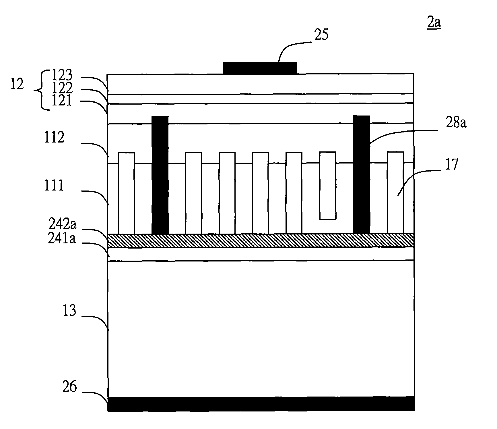
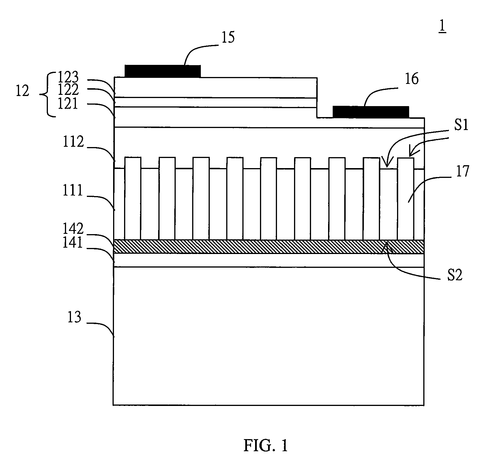
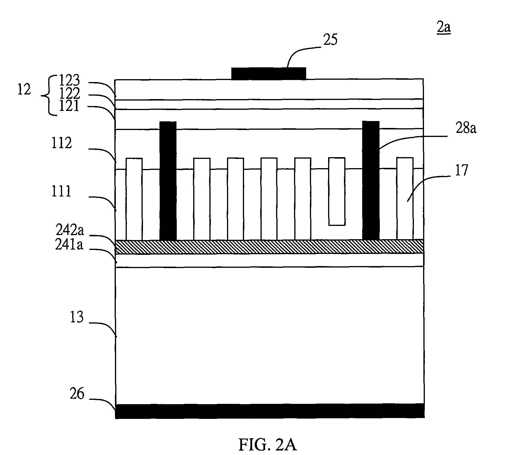
[0021]FIG. 1 shows the cross-sectional view of a horizontal light-emitting device 1 in accordance with an embodiment of the present disclosure. The light-emitting device 1 includes a thinned substrate 111 having a top surface S1 and a lower surface S2, a semiconductor buffer layer 112 deposed on the top surface S1, a semiconductor light-emitting structure 12 deposed on the semiconductor buffer layer 112 including a first-type conductivity semiconductor layer 121, an active layer 122, and a second-type conductivity semiconductor layer 123, wherein part of the semiconductor light-emitting structure 12 is removed to expose part of the first-type conductivity semiconductor layer 121, a reflective layer ...


PUM


Abstract

A semiconductor light-emitting device having a thinned structure comprises a thinned structure formed between a semiconductor light-emitting structure and a carrier. The manufacturing method comprises the steps of forming a semiconductor light-emitting structure above a substrate; attaching the semiconductor light-emitting structure to a support; thinning the substrate to form a thinned structure; forming or attaching a carrier to the thinned substrate; and removing the support.

Description

BACKGROUND OF THE DISCLOSURE[0001]1. Technical Field[0002]This disclosure relates to a light-emitting device having a thinned structure and the manufacturing method thereof.[0003]2. Description of the Related Art[0004]Semiconductor light-emitting devices such as light-emitting diode (LED) have continuing improvement in brightness recently, and the applied field is expanded from conventional signals or decorative use to light sources for various apparatus. Even in the coming future, it is possible for LEDs to replace the traditional fluorescent lamps as the new generational light source in the illuminating field.[0005]Currently the internal quantum efficiency (IQE) of light-emitting diode is about 50% to 80%, and about 20% to 50% of the input power can not be transferred into light but heat generated in the light-emitting diode. When the heat can not be dissipated from the light-emitting diode effectively, the heat results in temperature rising in the light-emitting diode, and the re...

Claims


Application Information

Patent Timeline
Patent Type & Authority Patents(United States)
IPC IPC(8): H01L27/15H01L31/12H01L33/00
CPCH01L33/0079H01L33/382H01L33/387H01L33/642H01L33/0093
Inventor HSIEH, MIN-HSUNLU, CHIH-CHIANGWANG, CHIEN-YUANCHEN, YEN-WENYEH, JUI-HUNGHUNG, SHIH-CHINTU, YU-WEIWU, CHUN-YIPENG, WEI-CHIH
Owner EPISTAR CORP
Why Eureka
Try Eureka