

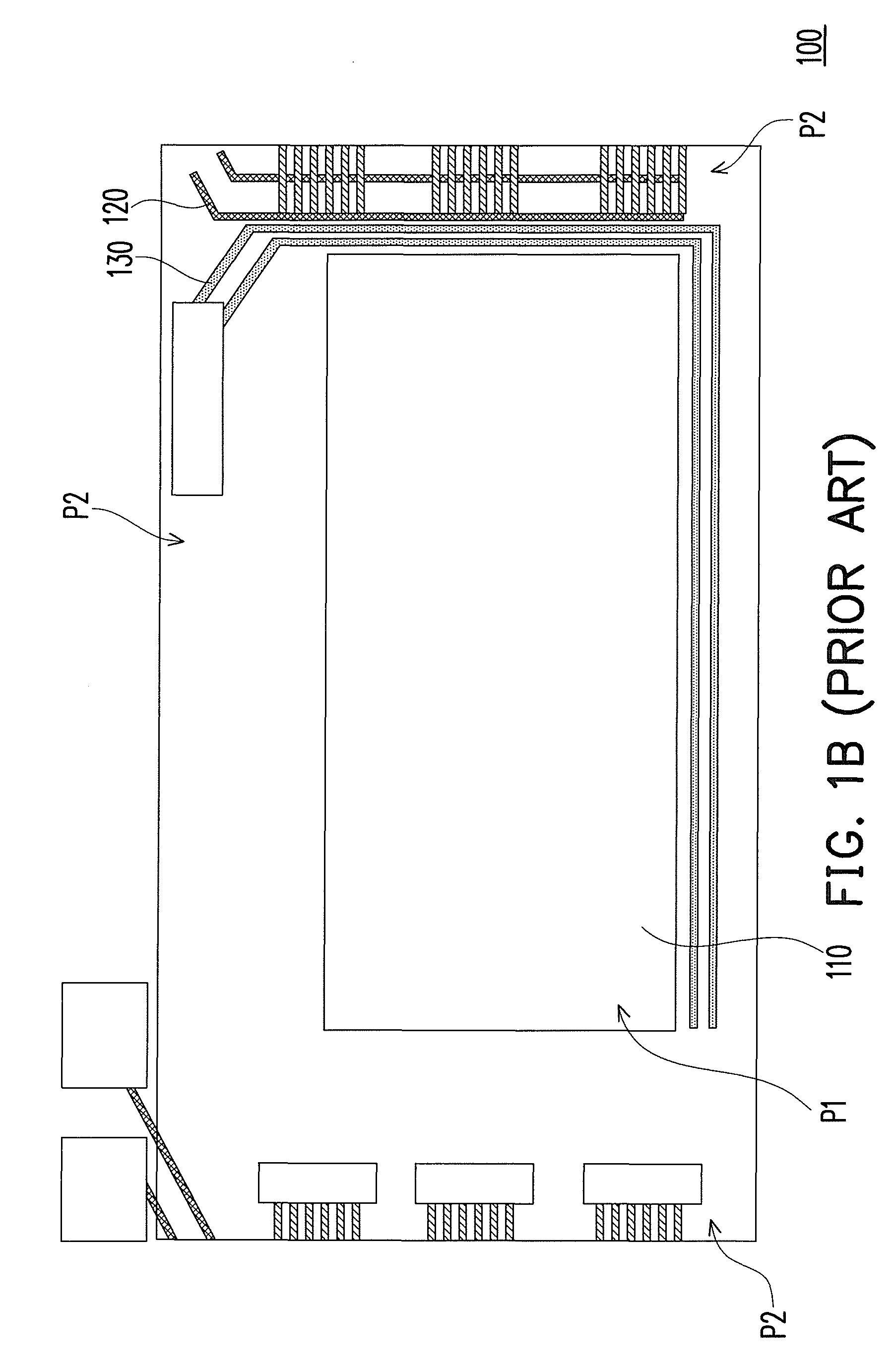
Array substrate with test shorting bar and display panel thereof
a technology of array substrate and shorting bar, applied in the field of substrates, can solve the problems of abnormal alignment, machine failure to catch the alignment, drastic competition of array substrate, etc., and achieve the effect of increasing the utilization of substra
- Summary
- Abstract
- Description
- Claims
- Application Information
AI Technical Summary
Benefits of technology
Problems solved by technology
Method used
Image

Examples
first embodiment
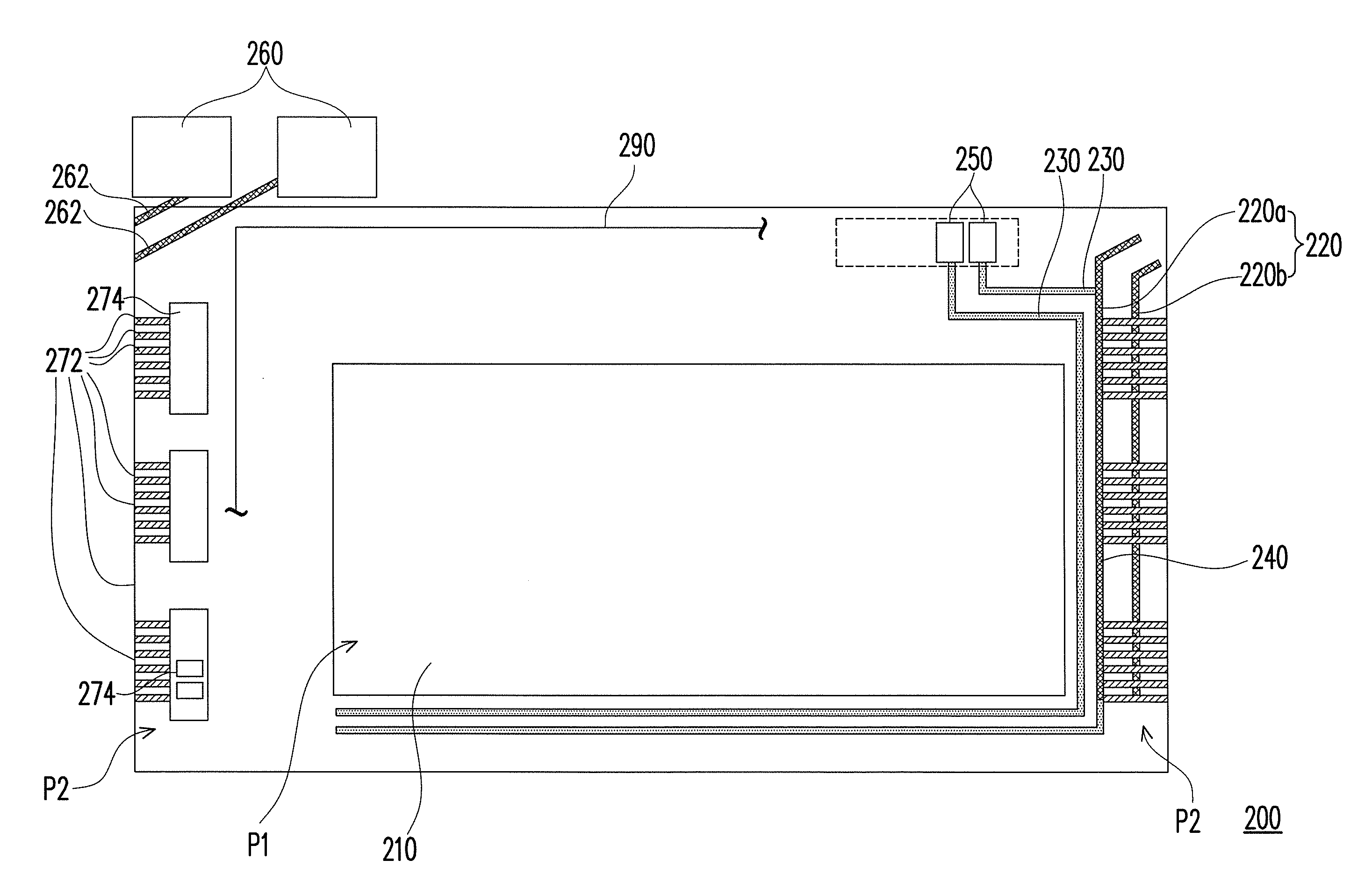
[0032]FIG. 2A is a top view illustrating an array substrate in the first embodiment of the present invention. Referring to FIG. 2A, an array substrate 200 comprises a display region P1 and a peripheral circuit region P2 adjacent to the display region P1. The array substrate 200 comprises a pixel array 210, a plurality of test shorting bars 220, and a plurality of wires 230 (for example, repair lines or repair wires). The test shorting bars 220 are usually used for detecting whether the arrays on a mother substrate (not shown) is electrically connected or disconnected (for example, short circuit or open-circuited). The pixel array 210 is disposed in the display region P1. The test shorting bars 220 and the wires 230 are disposed in the peripheral circuit region P2, and the wires 230 are electrically connected with the pixel array 210.
[0033]Additionally, the test shorting bars 220 can be divided into at least two types 220a and 220b, wherein at least one wire 230 and one of the test s...
second embodiment
[0043]FIG. 3 is a top view illustrating an array substrate in the second embodiment of the present invention. Referring to FIGS. 2A and 3, the array substrate 200 is similar to the array substrate 300, and the descriptions for the similarities are not repeated here. The array substrate 300 in this embodiment comprises a contact window 280. One of the first signal source connection wires 232a of the wires 230 is connected with the corresponding test shorting bars 220a through the contact window 280. Each wire 230 and each test shorting bar 220 share a part which forms the common trace 240, as shown in FIG. 3. In other words, one of the first signal source connection wires 232a of the wires 230 is electrically connected with the common trace 240 by the contact window 280, and the common traces 240 are electrically connected with pixel array connection wires 234. In this embodiment, each wire 230 and each test shorting bar 220 share a part for electrically connecting with each other.
[0...
third embodiment
[0047]FIG. 4 is a top view illustrating an array substrate in the third embodiment of the present invention. Referring to FIGS. 2A and 4, an array substrate 400 is similar to the array substrate 200, and the descriptions for the similarities are not repeated here. In this embodiment, the wires 230′ further comprise second signal source connection wires 236, wherein the wires 230′ are also called gate signal wires. It is to say that the wires 230′ are also used for transmitting the driving signals generated by the gate driving circuits 274. In this embodiment, the wires 230′ are, for example, formed by the first signal source connection wires 232′, the common trace 240′, the pixel array connection wires 234′, and the second signal source connection wires 236, as shown in FIG. 4.
[0048]Specifically, one of the wires 230′ and the test shorting bar 220a are connected by the common trace 240′, as shown in FIG. 4. The second signal source connection wires 236 are electrically connected wit...
PUM
| Property | Measurement | Unit |
|---|---|---|
| size | aaaaa | aaaaa |
| thickness | aaaaa | aaaaa |
| yield rate | aaaaa | aaaaa |
Abstract
Description
Claims
Application Information