

Optical control device
a control device and optical control technology, applied in the direction of optical elements, optical waveguide light guides, instruments, etc., can solve the problems of high manufacturing cost, long delay time, and complex manufacturing process of three-dimensional periodic structures
- Summary
- Abstract
- Description
- Claims
- Application Information
AI Technical Summary
Benefits of technology
Problems solved by technology
Method used
Image

Examples
exemplary embodiment 1
[0073]An optical control device according to a first exemplary embodiment of the present invention is now described with reference to the drawings.
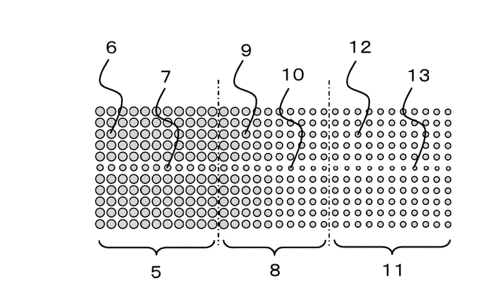
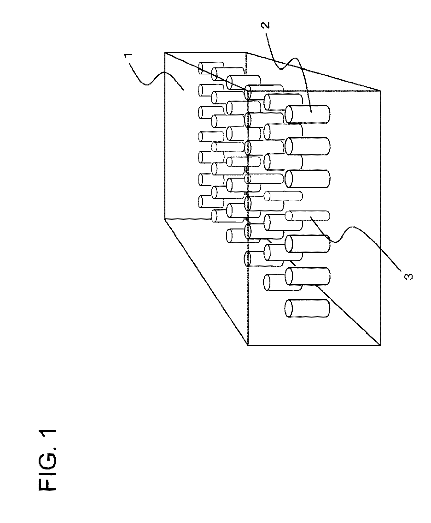
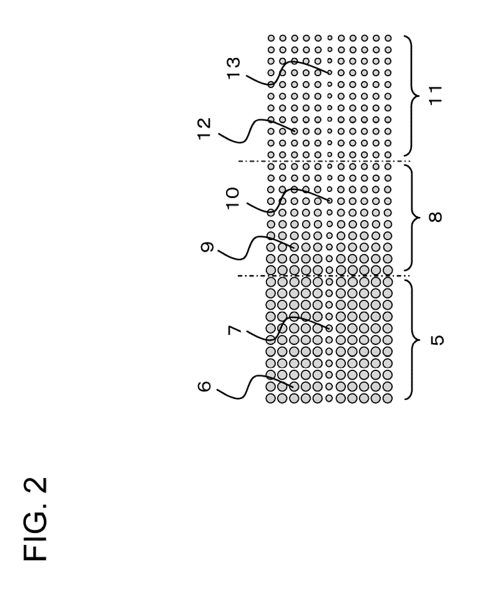
[0074]Referring to FIG. 2, an optical control device according to a preferred first exemplary embodiment of the present invention, usable as an optical delay element, is comprised of a pillar-shaped square-lattice photonic crystal. This photonic crystal includes a multiplicity of pillars of a dielectric material of a finite height in which there is provided a line-defect waveguide. The optical control device includes a first line-defect waveguide 5, a second line-defect waveguide 11 and a third line-defect waveguide 8. The second line-defect waveguide 11, as a line-defect waveguide in a square-lattice photonic crystal, is provided with a multiplicity of pillars thinner than the dielectric pillars of the first line-defect waveguide. The third line-defect waveguide 8 is provided with dielectric pillars, the thickness (cross-sectional area) ...
exemplary embodiment 2
[0085]In a second exemplary embodiment of the present invention, a light control element has a line-defect waveguide in a pillar-shaped square-lattice photonic crystal provided with a multiplicity of dielectric pillars that have a finite height, as shown in FIG. 5. The optical control device includes a first line-defect waveguide 32, a second line-defect waveguide 38 and a third line-defect waveguide 35. The second line-defect waveguide 38 is a line-defect waveguide in a square-lattice photonic crystal, which includes dielectric pillars 39, 40 differing in cross-sectional shape from dielectric pillars 33, 34 of the first line-defect waveguide 32. The third line-defect waveguide 35 includes dielectric pillars 36, 37. The cross-sectional shapes of the dielectric pillars 36 is(are) gradually varied from the cross-sectional shapes of the dielectric pillars 33 of the first line-defect waveguide 32 to those of the dielectric pillars 39 of the second line-defect waveguide 38 along the wave...
exemplary embodiment 3
[0093]A third exemplary embodiment of the present invention is directed to an optical control device, in particular an optical delay element which is comprised of a pillar-type square-lattice photonic crystal that has dielectric pillars with a finite height, and also has a line defect, as shown in FIG. 8. The optical control device includes a first line-defect waveguide 59, a second line-defect waveguide 65 and a third-line-defect waveguide 62. The second line-defect waveguide 65 is made up of dielectric pillars 66 and 67. The dielectric pillars 66 have lattice-point intervals, that is, local lattice constants, different from those of dielectric pillars 60 of the first line-defect waveguide 59, and the dielectric pillars 67 have lattice point intervals, that is, local lattice constants, different from those of dielectric pillars 61 of the first line-defect waveguide 59. The third line-defect waveguide 62 is interposed between the first line-defect waveguide 59 and the second line-de...
PUM
 Abstract
Description
Claims
Application Information