Package, method of manufacturing a package and frame
a packaging and frame technology, applied in the field of packaging, can solve the problems of reducing the overall package size and packages may have a standard and accepted footprint, and achieve the effect of uniform design and reduced frame costs
- Summary
- Abstract
- Description
- Claims
- Application Information
AI Technical Summary
Benefits of technology
Problems solved by technology
Method used
Image
Examples
first embodiment
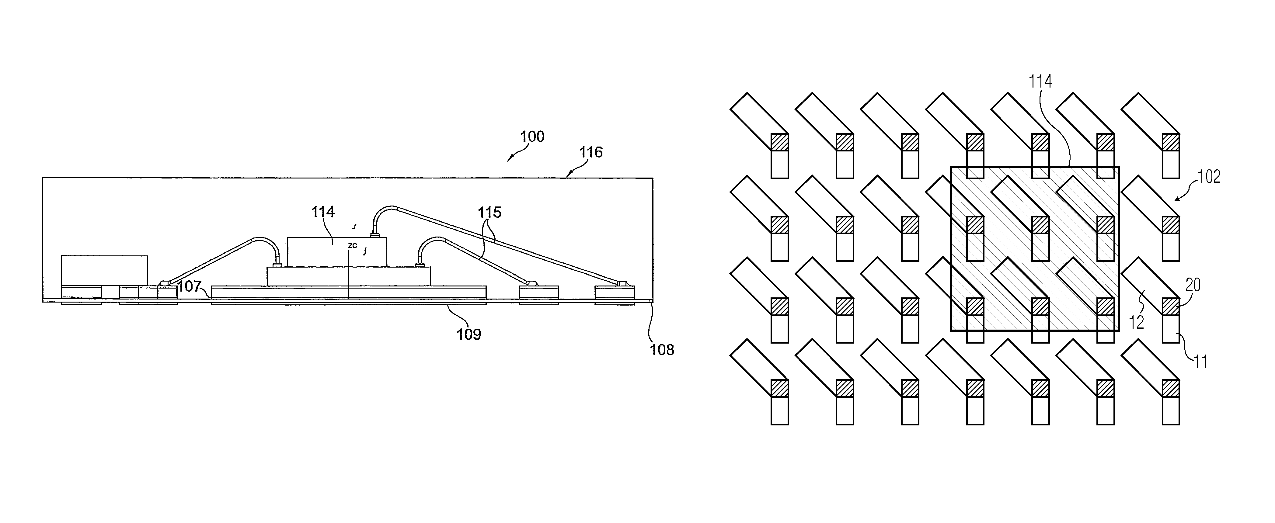
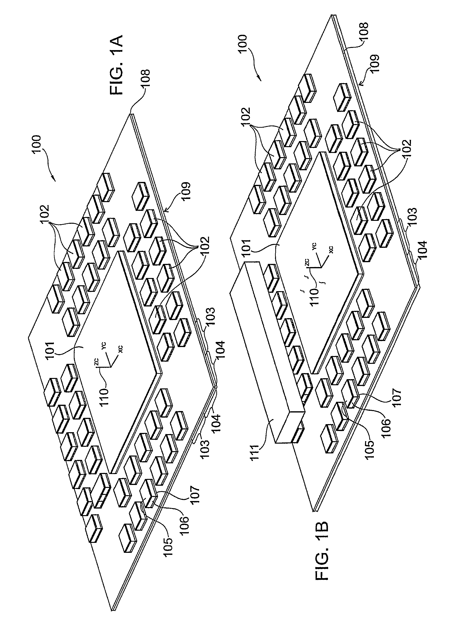
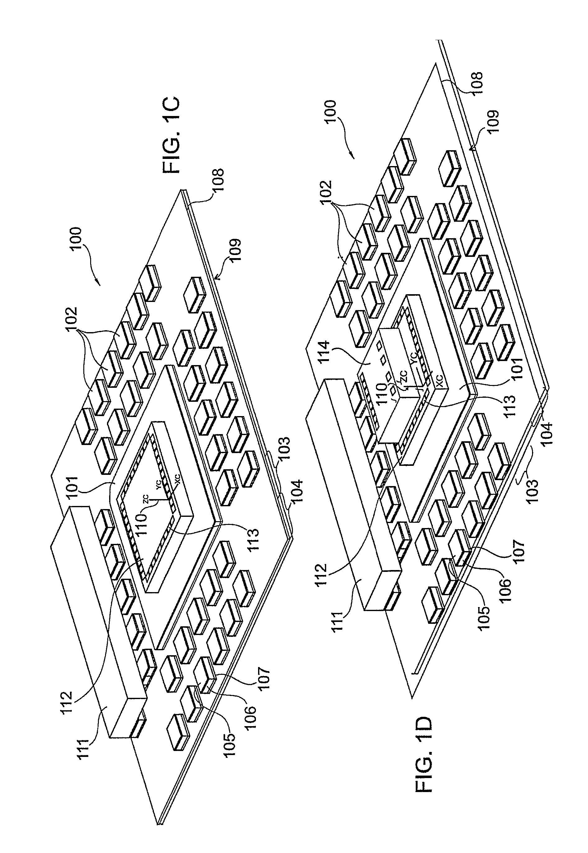
[0050]FIG. 3 shows diagramatically the invention in a top view. Several features are left out in FIG. 3 to improve the understanding, such as bonding wires and encapsulation. The Figure particularly shows the carrier 100 with frame contact pads 102 and the chip 114. The carrier is divided into a die attach area and an area outside the die attach area. As will be clear from the FIG. 3, it is one of the advantages of the present invention that the die attach area need not to be defined specifically. In fact, the die attach area is herein nothing else than the area of the carrier covered by the chip. In case the chip 114 is replaced by a chip of another size, the die attach area will change accordingly.
[0051]The frame contact pads 102 have a repetitive pattern 10 defined in the first conductive layer 106 of the carrier 100. The shaded part 20 therein refers to the terminal, that is exposed from the encapsulation. As indicated with reference to FIGS. 2A-G, the terminals are defined in t...
third embodiment
[0056]FIG. 5 diagrammatically shows the universal leadframe according to the invention. The FIG. 5 is schematical in the same manner as FIG. 3, i.e. it does not show the encapsulation or bond wires. This embodiment differs from the embodiments of FIGS. 3 and 4, in that not all the frame contact pads 102 have the same orientation. Each of the contact pads 102 has a first and a second flange 11, 12 that mutually enclose an angle of approximately 135 degrees. In this example, the first flange has a larger width than the second flange. An additional bulge is possible so as to provide sufficient overlap between the feature 10 in the first layer 106 and the terminal 20 defined in the second layer 108. A first and a second contact pad 120X, 120Y are mutually positioned such that their first flanges 11 face each other. This is deemed beneficial for the provision of interconnects between the two pads with bondwires, and also for the provision of discrete components such as diodes, capacitors...
PUM
| Property | Measurement | Unit |
|---|---|---|
| angle | aaaaa | aaaaa |
| thickness | aaaaa | aaaaa |
| thickness | aaaaa | aaaaa |
Abstract
Description
Claims
Application Information


