Magnetoresistive effect device and magnetic memory

a magnetic memory and magnetoresistive effect technology, applied in solid-state devices, magnetic bodies, instruments, etc., can solve the problems of requiring a greater magnetic field, and reducing the current flow through the wiring, so as to minimize the leakage magnetic field

Active Publication Date: 2012-07-17
KIOXIA CORP
View PDF12 Cites 26 Cited by
  • Summary
  • Abstract
  • Description
  • Claims
  • Application Information

AI Technical Summary

Benefits of technology

[0017]The present invention has been made in view of these circumstances, and an object of the present invention is to provide a magnetoresistive effect device that is capable of minimizing the leakage magnetic field applied to the storage layer, and a magnetoresistive access memory that includes the magnetoresistive effect device.

Problems solved by technology

A larger magnetic field can be generated from a larger amount of current, but the amount of current that can flow through the wirings is restricted due to miniaturization of devices.
However, a greater magnetic field is required for reversing the magnetization of a magnetic body due to miniaturization.
Therefore, it is very difficult to restrict the amount of current to a small value and achieve miniaturization at the same time.
As described above, it is very difficult to restrict the amount of current to a small value and achieve miniaturization at the same time, since the reversal magnetic field is increased by the increase of the magnetic energy of the magnetic body.
As a result, the cell area becomes relatively large, and it is impossible to realize miniaturization, a smaller amount of current, and a reduction in cell area at the same time.
In this magnetization reversing technique involving a spin-polarized current, however, the problem of thermal agitation becomes prominent with further miniaturization.
Also, the storage layer having smaller coercive force than the reference layer is greatly affected by the leakage magnetic field from the reference layer.
More specifically, due to the influence of the leakage magnetic field from the reference layer, the amount of reversal current required for writing is increased, and the thermal stability becomes poorer.
However, if the SAF structure is of a perpendicular magnetization type, a film thickness ratio of approximately 1.2 cannot sufficiently reduce the leakage magnetic field applied to the storage layer, as discovered by the inventors and will be described later.

Method used


Image

  • Magnetoresistive effect device and magnetic memory
  • Magnetoresistive effect device and magnetic memory
  • Magnetoresistive effect device and magnetic memory

Examples


first embodiment

(First Embodiment)

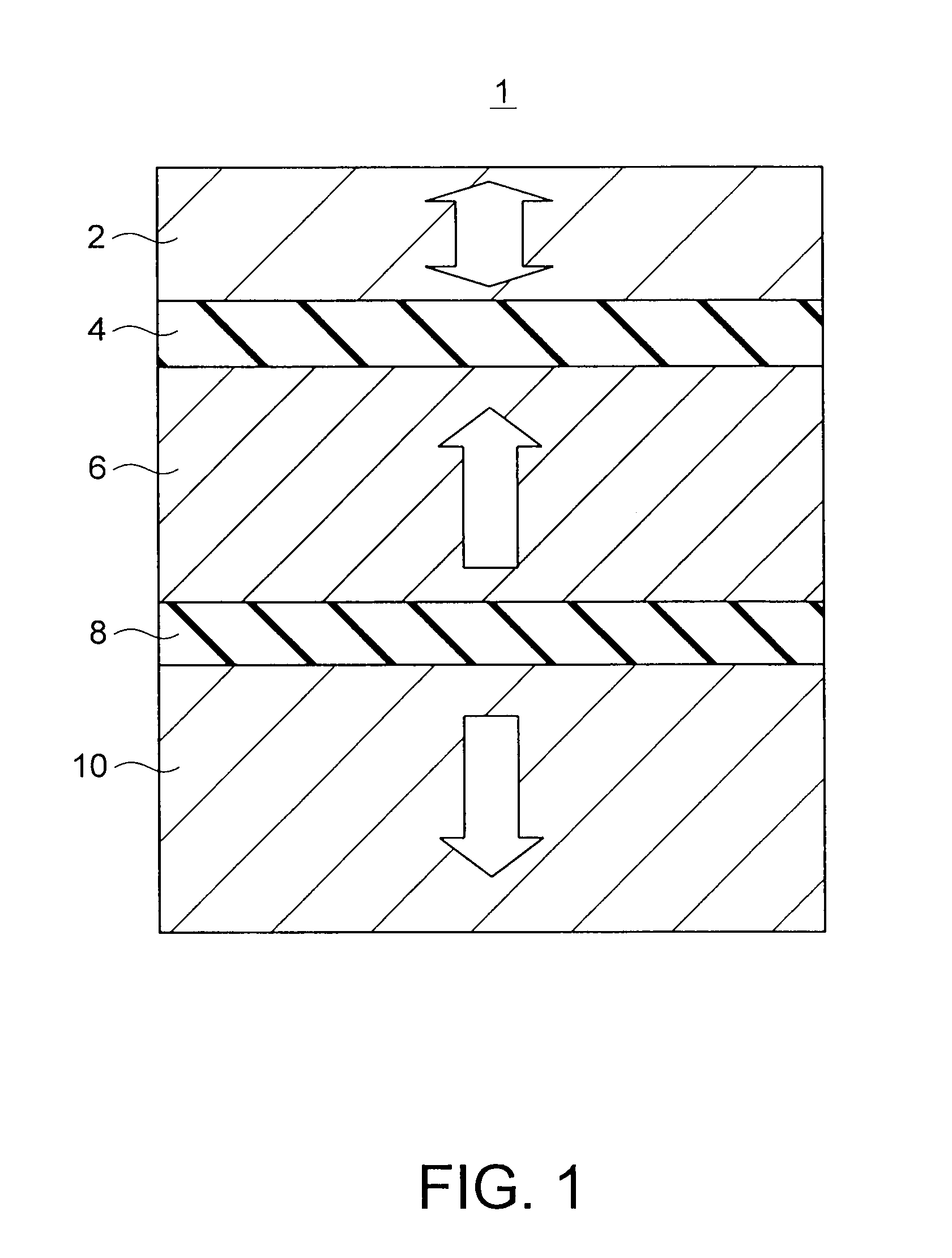
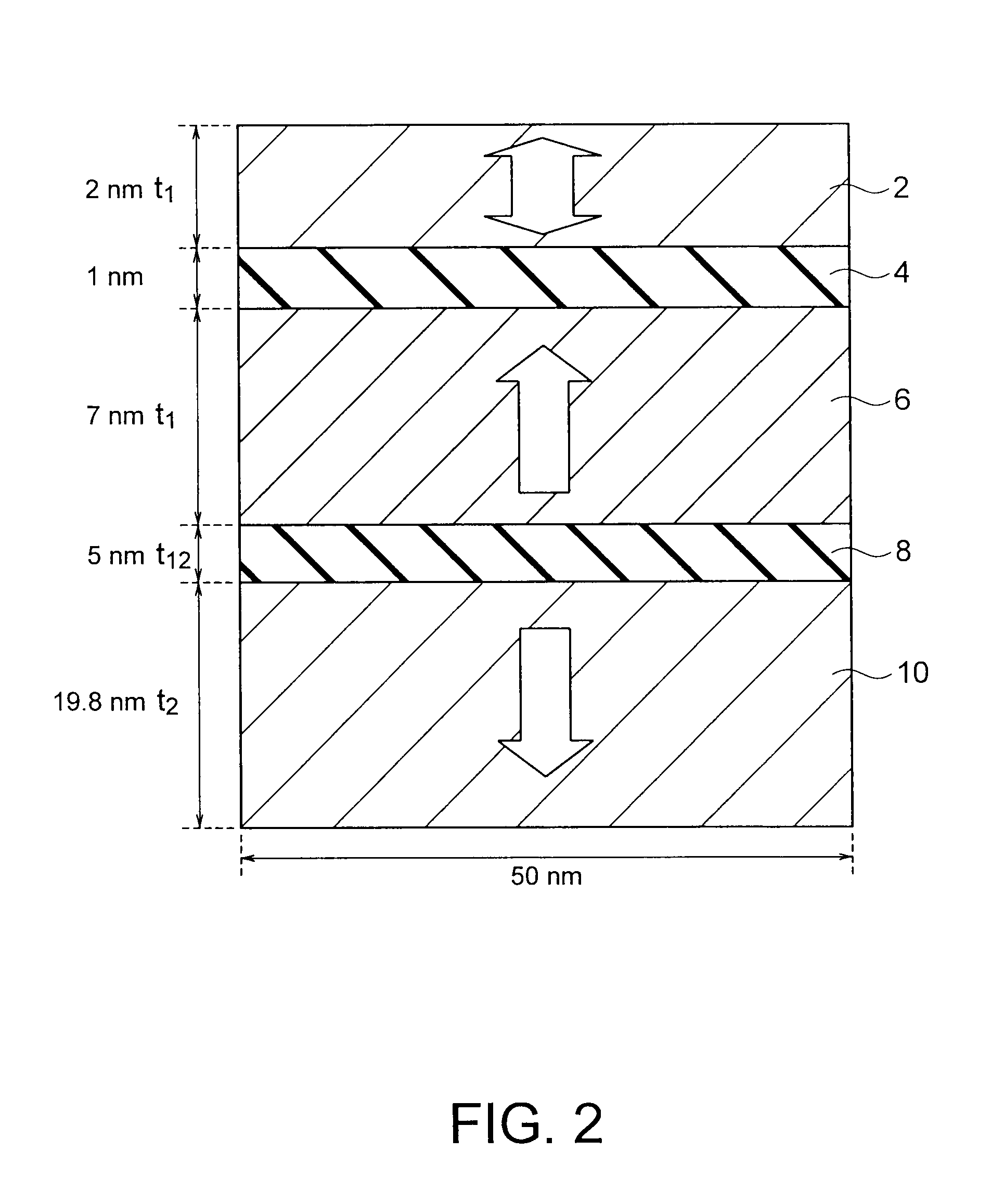
[0049]FIG. 1 shows a magnetoresistive effect device in accordance with a first embodiment of the present invention. The magnetoresistive effect device of this embodiment is a MTJ device 1 of a single-pin structure. The MTJ device 1 of this embodiment has a stacked structure that includes a free magnetization layer (a storage layer) 2 formed with a magnetic layer, a reference layer 6 formed with a magnetic layer, a ferromagnetic layer 10 formed with a magnetic layer, a nonmagnetic layer 4 interposed between the storage layer 2 and the reference layer 6, and a nonmagnetic layer 8 interposed between the reference layer 6 and the ferromagnetic layer 10. Accordingly, the MTJ device 1 of this embodiment may be a stacked structure formed by stacking the ferromagnetic layer 10, the nonmagnetic layer 8, the reference layer 6, the nonmagnetic layer 4, and the storage layer 2 in this order (the stacked structure formed in the order illustrated in FIG. 1), or may be a stacked ...

second embodiment

(Second Embodiment)

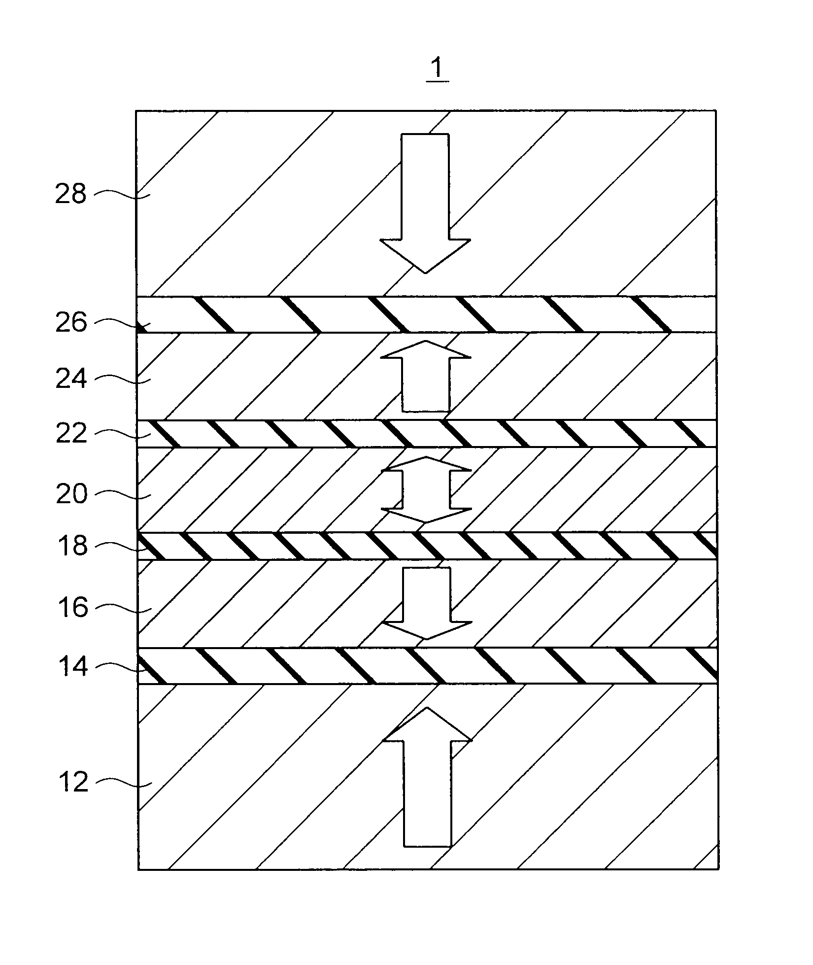
[0111]FIG. 11 shows a magnetoresistive effect device in accordance with a second embodiment of the present invention. The magnetoresistive effect device of this embodiment is a MTJ device 1 of a dual-pin structure. The MTJ device 1 of this embodiment has a stacked structure that is formed by stacking a ferromagnetic layer 12, a nonmagnetic layer 14, a reference layer 16, a nonmagnetic layer 18, a storage layer 20, a nonmagnetic layer 22, a reference layer 24, a nonmagnetic layer 26, and a ferromagnetic layer 28 in this order. Alternatively, the MTJ device 1 of this embodiment may have a stacked structure that is formed by stacking the ferromagnetic layer 28, the nonmagnetic layer 26, the reference layer 24, the nonmagnetic layer 22, the storage layer 20, the nonmagnetic layer 18, the reference layer 16, the nonmagnetic layer 14, and the ferromagnetic layer 12 in this order, which is the reverse order of the order illustrated in FIG. 11.

[0112]The reference layers 1...

third embodiment

(Third Embodiment)

[0137]FIG. 13 shows a magnetoresistive effect device in accordance with a third embodiment of the present invention. The magnetoresistive effect device of this embodiment is a MTJ device 1 of a single-pin structure. The MTJ device 1 of this embodiment has a stacked structure that includes a storage layer 102 formed with a magnetic layer, a reference layer 106 formed with a magnetic layer, a ferromagnetic layer 110 formed with a magnetic layer, a nonmagnetic layer 104 interposed between the storage layer 102 and the reference layer 106, and an antiferromagnetic layer 108 interposed between the reference layer 106 and the ferromagnetic layer 110. Accordingly, the MTJ device 1 of this embodiment may be a stacked structure formed by stacking the storage layer 102, the nonmagnetic layer 104, the reference layer 106, the antiferromagnetic layer 108, and the ferromagnetic layer 110 in this order (the stacked structure formed in the order illustrated in FIG. 13), or may be...


PUM


Abstract

A magnetic memory includes a magnetoresistive effect device comprising: a first ferromagnetic layer that has magnetic anisotropy in a direction perpendicular to a film plane thereof; a first nonmagnetic layer that is provided on the first ferromagnetic layer; a first reference layer that is provided on the first nonmagnetic layer, has magnetic anisotropy in a direction perpendicular to a film plane thereof, has magnetization antiparallel to a magnetization direction of the first ferromagnetic layer, and has a film thickness that is 1 / 5.2 to 1 / 1.5 times as large as a film thickness of the first ferromagnetic layer in the direction perpendicular to the film plane; a second nonmagnetic layer that is provided on the first reference layer; and a storage layer that is provided on the second nonmagnetic layer, has magnetic anisotropy in a direction perpendicular to a film plane thereof, and has a magnetization direction varied by spin-polarized electrons caused by flowing the current to the magnetoresistive effect device.

Description

CROSS-REFERENCE TO RELATED APPLICATION[0001]This application is based upon and claims the benefit of priority from prior Japanese Patent Applications Nos. 2008-248633 and 2009-78799 filed on Sep. 26, 2008 and Mar. 27, 2009 respectively in Japan, the entire contents of which are incorporated herein by reference.BACKGROUND OF THE INVENTION[0002]1. Field of the Invention[0003]The present invention relates to a magnetoresistive effect device that is capable of recording information with a supply of bidirectional current, and a magnetic memory that includes the magnetoresistive effect device.[0004]2. Related Art[0005]A magnetoresistive random access memory (MRAM) that utilizes a tunneling magneto Resistive (TMR) effect characteristically stores data depending on the magnetization states of MTJ (Magnetic Tunnel Junction) devices. Generally, a MTJ device includes a magnetic layer called a storage layer, another magnetic layer called a reference layer, and a tunnel barrier layer interposed ...

Claims


Application Information

Patent Timeline
Patent Type & Authority Patents(United States)
IPC IPC(8): G11C11/00
CPCB82Y25/00G11C11/16H01F10/3254H01F10/3277H01L43/08H01F10/3286H01F10/329H01L27/228H01F10/123G11C11/161G11C11/5607H10B61/22H10N50/10
Inventor OZEKI, JYUNICHISHIMOMURA, NAOHARUIKEGAWA, SUMIOKAI, TADASHINAKAYAMA, MASAHIKOAIKAWA, HISANORIKISHI, TATSUYAYODA, HIROAKIKITAGAWA, EIJIYOSHIKAWA, MASATOSHI
Owner KIOXIA CORP
Why Eureka
Try Eureka