Card edge connector

a card edge connector and connector technology, applied in the direction of coupling device connection, connection contact member material, coupling protective earth/shielding arrangement, etc., can solve the problem of reducing the efficiency of data transfer through the card edge connector

Active Publication Date: 2012-07-31
TE CONNECTIVITY CORP
View PDF13 Cites 37 Cited by
  • Summary
  • Abstract
  • Description
  • Claims
  • Application Information

AI Technical Summary

Benefits of technology

[0004]In one embodiment, a card edge connector is provided for mating with a printed circuit board (PCB) having a card edge. The connector includes a housing having an elongate card slot and a mounting side. The card slot extends a slot length and is configured to receive the card edge of the PCB therein. The mounting side extends a side length and a width. The side length of the mounting side extends in a direction that extends along a direction of the slot length of the card slot. Signal contacts are held by the housing. The signal contacts include first signal contacts and second signal contacts. The first and second signal contacts have respective first and second signal mounting segments that are arranged in first and second signal rows, respectively, that extend along the side length of the mounting side of the housing. The first and second signal rows are spaced apart from each other along the width of the mounting side. Ground contacts are held by the housing. The ground contacts include ground mounting segments arranged in a ground row that extends along the side length of the mounting side. The ground row extends between the first and second signal rows along the width of the mounting side of the housing.

Problems solved by technology

But, the proximity of the ground contacts and ground contact pads to the differential pairs may reduce the impedance of signals transmitted through the differential pairs, which may reduce the efficiency of data transfer through the card edge connector.

Method used


Image

  • Card edge connector
  • Card edge connector
  • Card edge connector

Examples


Embodiment Construction

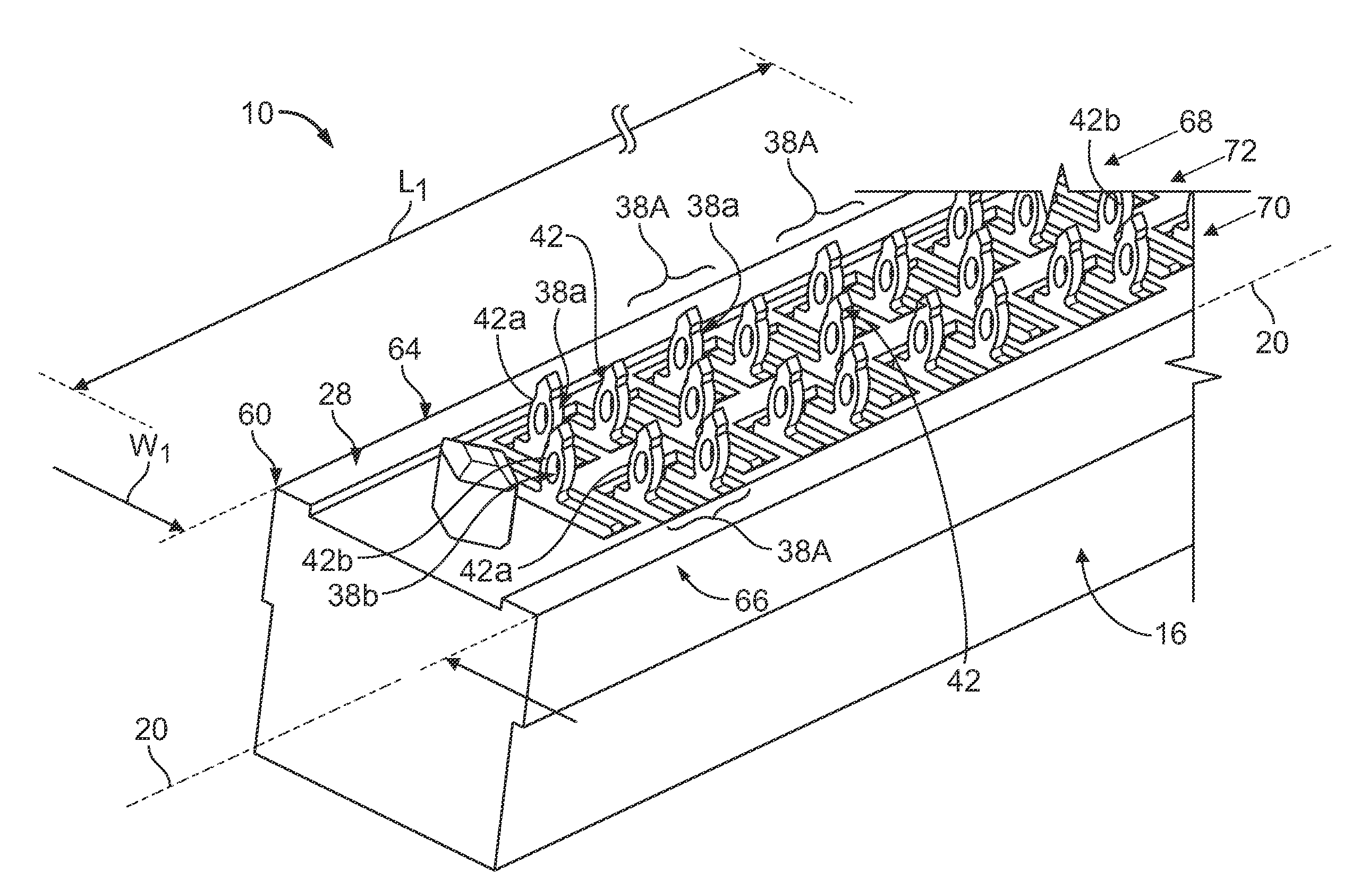
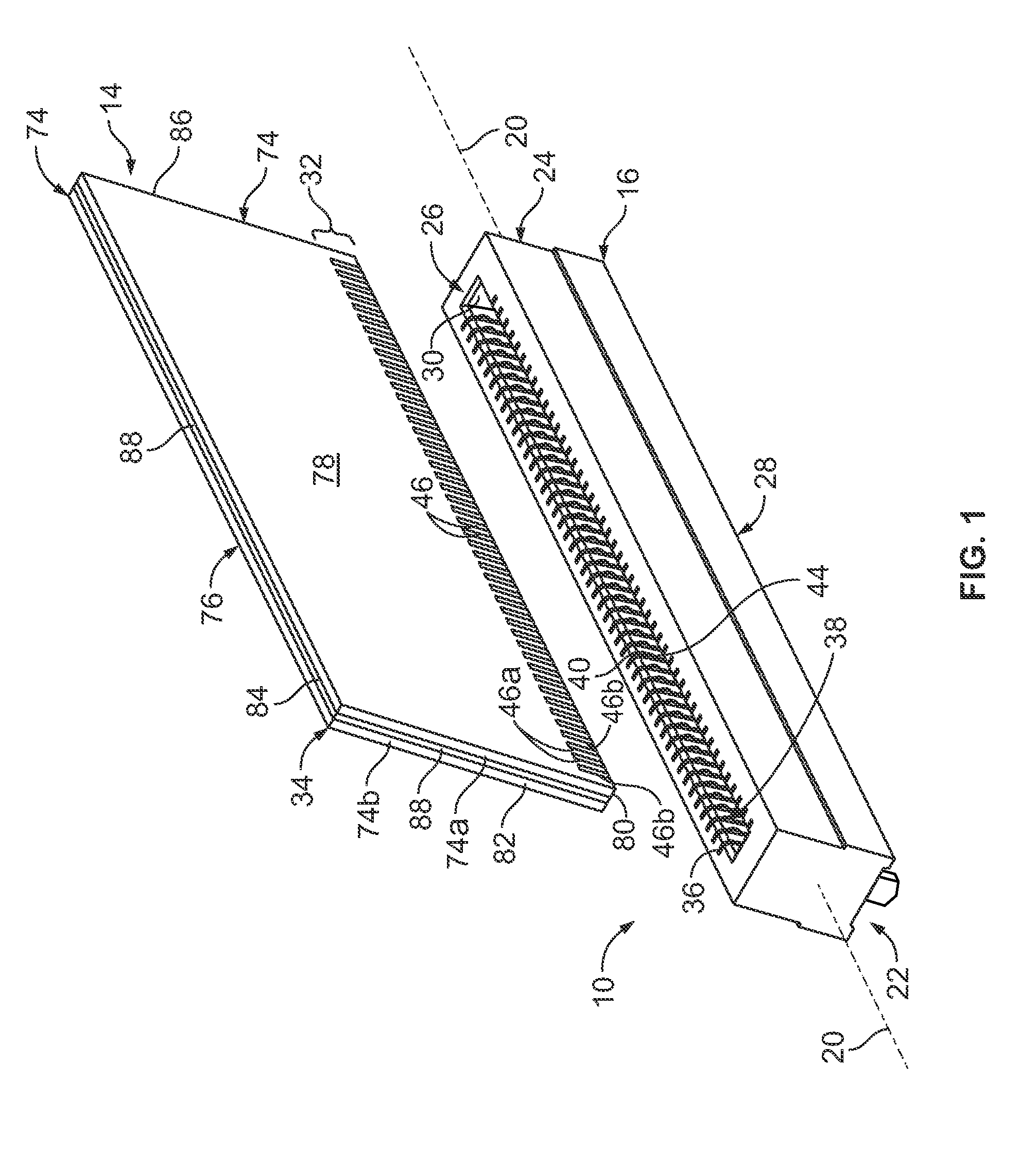
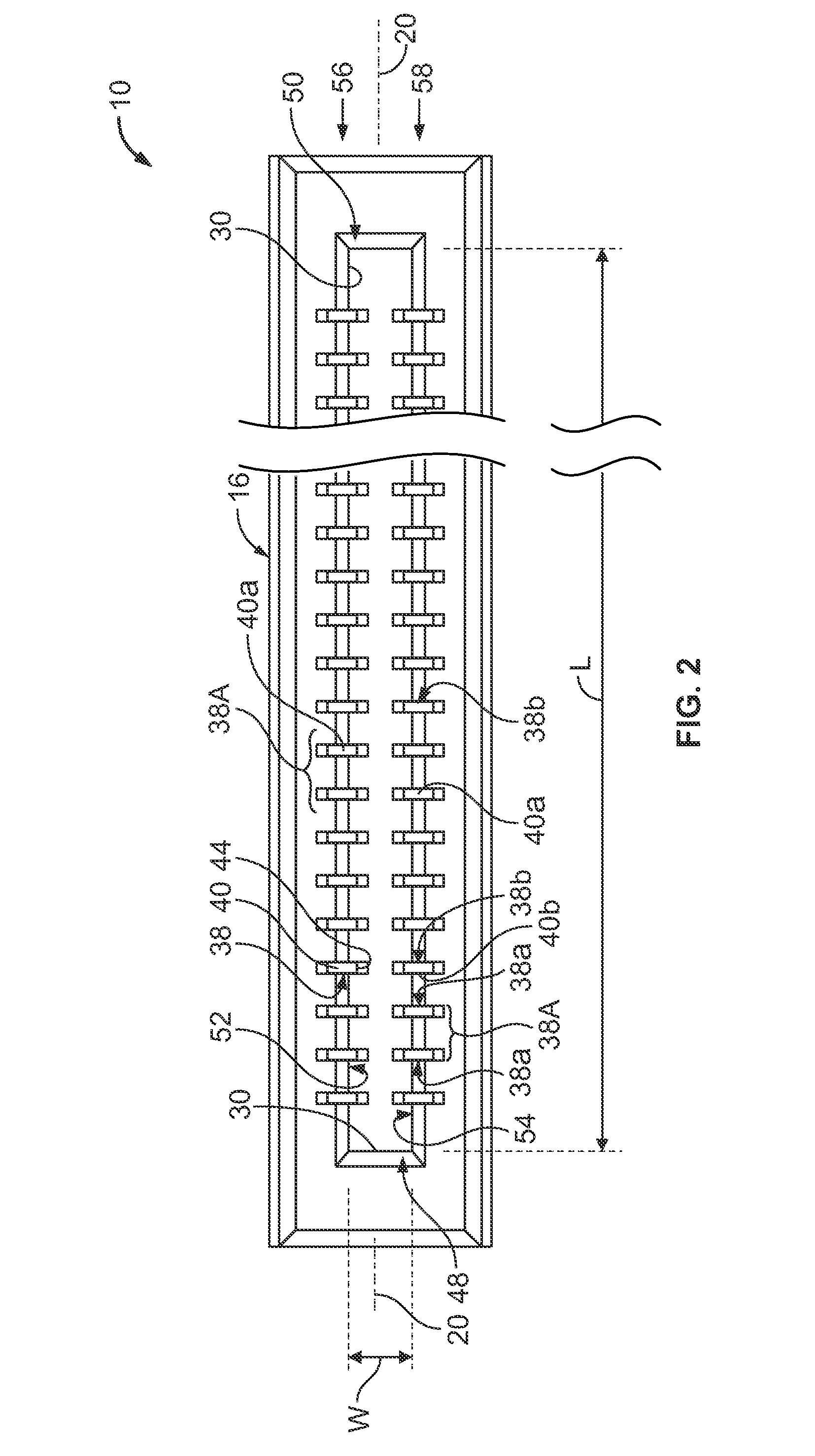
[0017]FIG. 1 is a partially exploded perspective view of an exemplary embodiment of a card edge connector 10 and a portion of an exemplary embodiment of an electronic module 14. The connector 10 includes a dielectric housing 16 that extends a length along a central longitudinal axis 20 from an end 22 to an opposite end 24. The housing 16 has a mating side 26 and a mounting side 28. The housing 16 includes a card slot 30 that is configured to receive a card edge 32 of the electronic module 14 therein. More specifically, the electronic module 14 includes a printed circuit board (PCB) 34 that includes the card edge 32. Only the PCB 34 of the electronic module 14 is shown in FIG. 1. As used herein, the term “printed circuit board” is intended to mean any electric circuit in which the electrical conductors have been printed or otherwise deposited in predetermined patterns on an electrically insulating substrate. A combination of the connector 10 and the electronic module 14 may be referr...


PUM


Abstract

A card edge connector is provided for mating with a printed circuit board (PCB) having a card edge. The connector includes a housing having an elongate card slot and a mounting side. The card slot extends a slot length and is configured to receive the card edge of the PCB therein. The mounting side extends a side length and a width. The side length of the mounting side extends in a direction that extends along a direction of the slot length of the card slot. Signal contacts are held by the housing. The signal contacts include first signal contacts and second signal contacts. The first and second signal contacts have respective first and second signal mounting segments that are arranged in first and second signal rows, respectively, that extend along the side length of the mounting side of the housing. The first and second signal rows are spaced apart from each other along the width of the mounting side. Ground contacts are held by the housing. The ground contacts include ground mounting segments arranged in a ground row that extends along the side length of the mounting side. The ground row extends between the first and second signal rows along the width of the mounting side of the housing.

Description

BACKGROUND OF THE INVENTION[0001]The subject matter described and / or illustrated herein relates generally to card edge connectors.[0002]Computers and servers use numerous types of electronic modules, such as processor and memory modules (e.g. Dynamic Random Access Memory (DRAM), Synchronous Dynamic Random Access Memory (SDRAM), or Extended Data Out Random Access Memory (EDO RAM), and the like). The memory modules are produced in a number of formats such as, for example, Single In-line Memory Modules (SIMM's), Dual In-line Memory Modules (DIMM's), Small Outline DIMM's (SODIMM's), Fully Buffered DIMM's, and the like. The electronic modules may be installed in card edge connectors that are mounted on a motherboard or other system board.[0003]Electronic modules often include a printed circuit board (PCB) having a card edge that is received within a card slot of the card edge connector. The PCB includes contact pads arranged along the card edge on two opposite sides of the PCB. The card ...

Claims


Application Information

Patent Timeline
Patent Type & Authority Patents(United States)
IPC IPC(8): H01R13/648
CPCH01R13/6471H01R12/721H01R12/737
Inventor WESTMAN, JOHN EUGENEMCMASTER, JR., BRIAN KEITHJACOBS, EDMUND LUTHERKNISELY, JR., EDWARD EUGENEKORDAS, ALAN ANTHONYCLEWELL, CRAIG WILLIAM
Owner TE CONNECTIVITY CORP
Why Eureka
Try Eureka