Electronic component package, electronic component mounted apparatus, method of inspecting bonding portion therein, and circuit board

a technology of electronic components and mounting devices, which is applied in the direction of sustainable manufacturing/processing, instruments, semiconductor/solid-state device details, etc., can solve the problems of defective the failure of external visual inspection, and the failure of the bonding between the external connection land to be defective, so as to improve the reliability of the bonding between the solder ball and the circuit board-side land, the effect of satisfactory

Active Publication Date: 2012-07-31
PANASONIC CORP
View PDF10 Cites 1 Cited by
  • Summary
  • Abstract
  • Description
  • Claims
  • Application Information

AI Technical Summary

Benefits of technology

[0019]Therefore, with the foregoing in mind, it is an object of the present invention to provide an electronic component mounted apparatus in which bonding failures between external connection lands and solder balls and between circuit board-side lands and the solder balls can be reduced, and the bonding state can be inspected easily, and a method of inspecting a bonding portion therein.
[0021]With this configuration, because the external connection land includes an arc portion, the molten solder ball that tends to form a circular shape due to surface tension wets without being deformed considerably, and therefore satisfactory bondability between the solder ball and the external connection land is obtained. Further, because the external connection land also includes a straight portion, the straight portion is displayed in an X-ray image, and the bondability between the solder ball and the external connection land can be inspected easily using X-rays. For this reason, the reliability of the bondability between the solder ball and the external connection land is improved.
[0023]With this configuration, because the circuit board-side land includes an arc portion, the solder ball of an electronic component package to be mounted wets without being deformed considerably, and satisfactory bondability between the solder ball and the circuit board-side land is obtained. Further, because the circuit board-side land also includes a straight portion, the straight portion is displayed in an X-ray image, and the bondability between the solder ball and the circuit board-side land can be inspected easily using X-rays. For this reason, the reliability of the bondability between the solder ball and the circuit board-side land is improved.
[0024]An electronic component mounted apparatus of the present invention includes the above-described electronic component package and above-described circuit board, wherein the solder ball is connected to the circuit board-side land. With this configuration, satisfactory bondability between the solder ball and the external connection land, and satisfactory bondability between the solder ball and the circuit board-side land are obtained. At the same time, the bondability between the solder ball and the external connection land and the bondability between the solder ball and the circuit board-side land can be inspected easily using X-rays.
[0025]A method of inspecting a bonding portion of an electronic component package of the present invention is a method of inspecting the bonding portion between the external connection land and the solder ball in the above-described electronic component package, wherein X-rays are irradiated on the solder ball and it is determined that the bonding portion between the external connection land and the solder ball in the electronic component package is satisfactory if a straight portion is included in the outer shape of the solder ball in an image formed based on X-rays that have passed through the solder ball. According to this method, the bonding state of the bonding portion between the external connection land and the solder ball can be determined easily by the presence of a straight portion of the external connection land.
[0026]A method of inspecting a bonding portion of an electronic component mounted apparatus is a method of inspecting the bonding portion between the external connection land and the circuit board-side land by the solder ball in the above-described electronic component mounted apparatus, wherein X-rays are irradiated on the solder ball and it is determined that at least one of the bonding portion between the external connection land of the electronic component package and the solder ball and the bonding portion between the circuit board-side land of the circuit board and the solder ball is satisfactory if a straight portion is included in the outer shape of the solder ball in an image formed based on X-rays that have passed through the solder ball. According to this method, the bonding state of the bonding portion between the external connection land and the solder ball can be determined easily. According to this method, the bonding state of the bonding portion between the external connection land and the circuit board-side land by the solder ball can be determined easily by the presence of a straight portion of the external connection land and the circuit board-side land.

Problems solved by technology

This phenomenon is difficult to detect by external visual inspection.
This defective solder wetting is caused by warping of the substrate due to heat generated during reflowing, weak activity of flux, random variations in solder ball size, or the like.
If the solder ball has poor wettability, the bonding between the circuit board-side land and the external connection land will be defective.
However, in this configuration, the cross sections i1 and i2 cannot be distinguished, and it is therefore difficult to determine the acceptability of the wettability.
Further, because the transmission cross sections of the land and the solder ball have a similar circular shape, the boundary or contour of each shape does not appear clearly in X-ray image density, and it is therefore further difficult to distinguish the cross sections i1 and i2.
Also, because the solder ball is spherical and the land is circular, an X-ray image is displayed in the shape of a circle regardless of whether or not the solder ball wets and spreads, and it is therefore difficult to determine the acceptability of wettability (bondability with the land).
This results in the problem that the occurrence of bonding failures between the circuit board-side land and the solder ball increases, and connection reliability is degraded.

Method used


Image

  • Electronic component package, electronic component mounted apparatus, method of inspecting bonding portion therein, and circuit board
  • Electronic component package, electronic component mounted apparatus, method of inspecting bonding portion therein, and circuit board
  • Electronic component package, electronic component mounted apparatus, method of inspecting bonding portion therein, and circuit board

Examples


embodiment 1

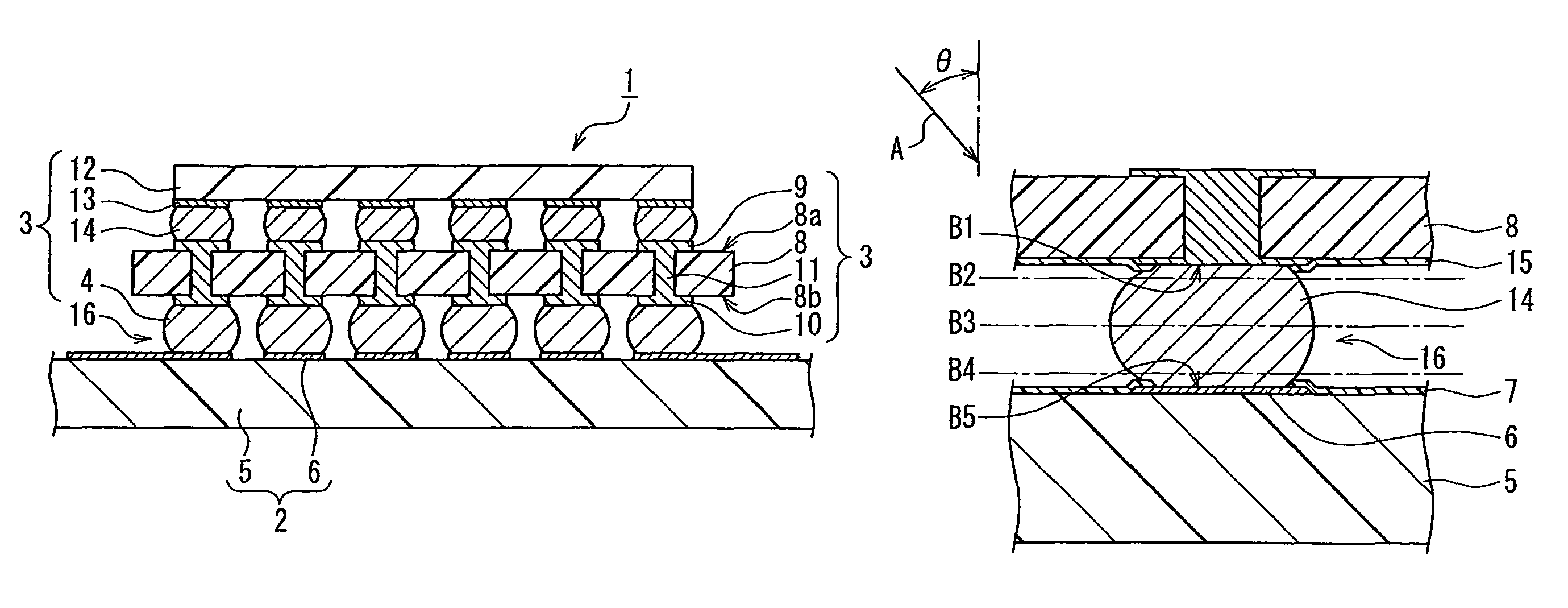
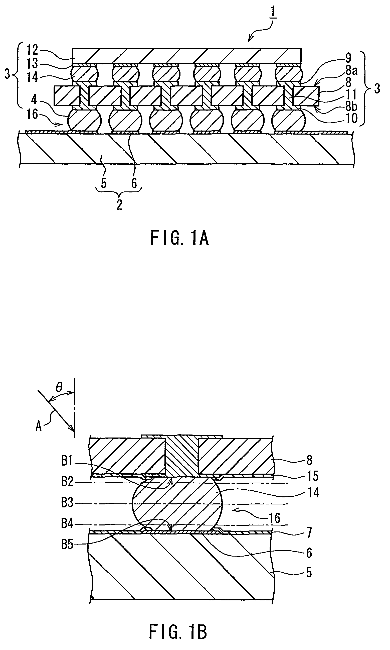
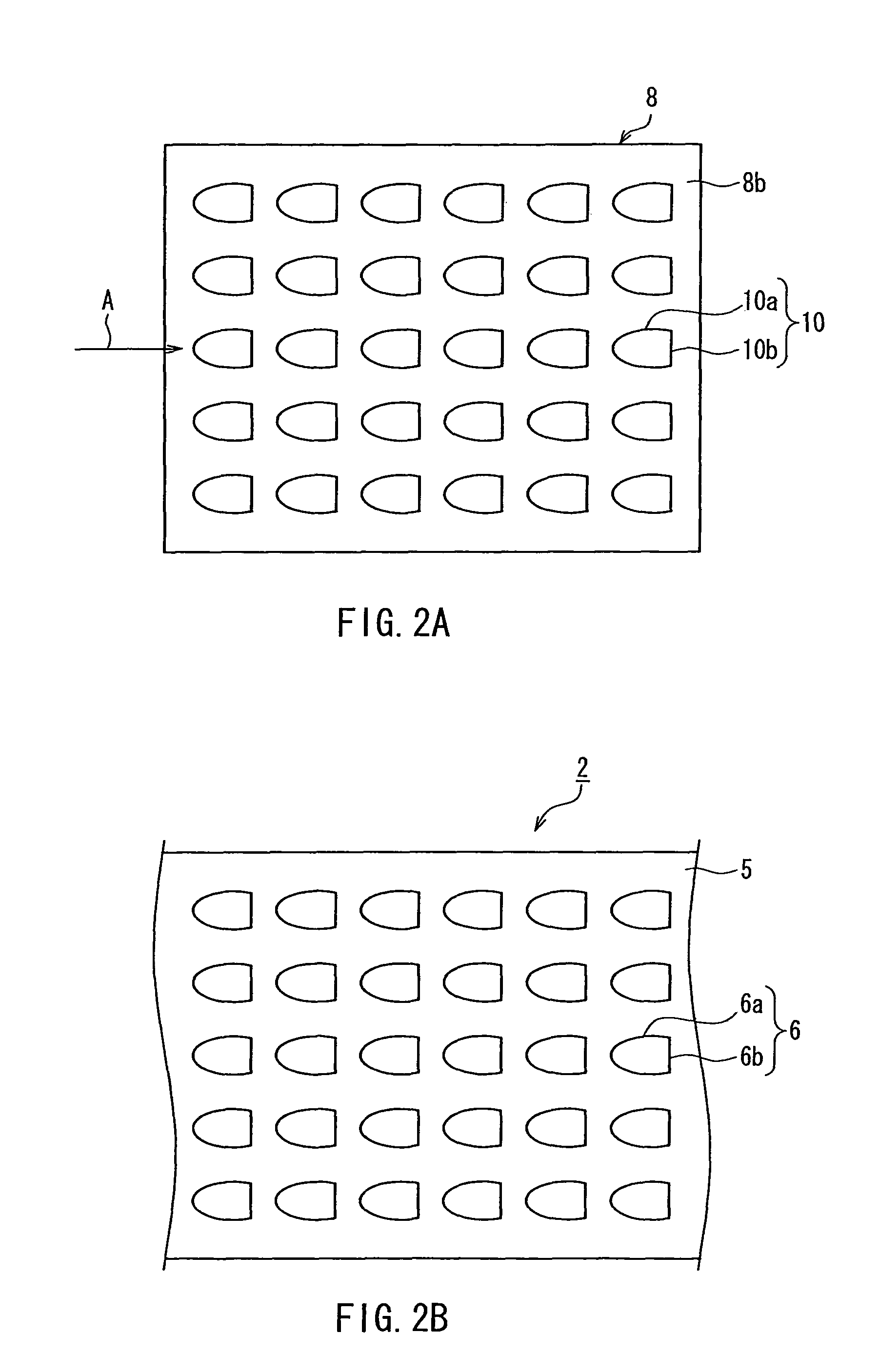
[0066]FIG. 1A is a cross-sectional conceptual diagram illustrating the configuration of an electronic component mounted apparatus 1 that includes an electronic component package 3 according to Embodiment 1 of the present invention. FIG. 1B is an enlarged cross-sectional conceptual diagram showing a part of FIG. 1A. The same reference numerals are assigned to elements having the same configuration, and some of the reference numerals are omitted. FIG. 2A is a conceptual diagram of the lower surface 8b of a carrier substrate according to the present embodiment. FIG. 2B is a conceptual diagram of a circuit board 2 according to the present embodiment. In FIGS. 2A and 2B, the same reference numerals are assigned to elements having the same configuration as those of FIGS. 1A and 1B, and some of the reference numerals are omitted.

[0067]As shown in FIG. 1A, the electronic component mounted apparatus 1 includes an electronic component package 3 mounted on a circuit board 2. The electronic com...

embodiment 2

[0104]FIG. 7 is a plan view illustrating the configuration of external connection lands 31 of a carrier substrate 8 of a semiconductor mounting apparatus according to Embodiment 2 of the present invention. The semiconductor mounting apparatus according to the present embodiment is the same as that of Embodiment 1, except that the external connection lands 31 have a configuration different from that of the external connection lands of Embodiment 1. In the semiconductor mounting apparatus of the present embodiment, the same reference numerals are assigned to elements having the same configuration as that of the semiconductor mounting apparatus of Embodiment 1, and thus their descriptions are omitted.

[0105]The external connection lands 31 have a rectangular shape whose corner portions are circular arc-shaped, that is, a shape that includes four arc portions and four straight portions that are connected to each other. With this configuration, molten solder balls 4, which tend to form a ...

embodiment 3

[0111]FIG. 10 is a plan view illustrating the configuration of an electronic component mounted apparatus 41 according to Embodiment 3 of the present invention. The electronic component mounted apparatus 41 includes an electronic component package 43 mounted on a circuit board 42. The circuit board 42 includes an insulating substrate made of an epoxy resin or the like, wirings (not shown) that are provided on the insulating substrate, and a resist that is disposed on the wirings and the circuit board 42. The wirings are made of copper or the like. Circuit board-side lands (not shown in FIG. 10) for connecting to the electronic component package 43 are formed on the end portion of the wirings.

[0112]The electronic component package 43 is a surface-mount type IC package that includes connection terminals for electrically connecting to the circuit board 42 that are provided in the bottom, and is packaged by, for example, BGA type or LGA type including a carrier substrate or the like CSP....


PUM


Abstract

An electronic component package includes: an insulating carrier substrate; a connection wiring that is provided on one side of the carrier substrate; an IC chip that is connected to the connection wiring; an external connection land that is disposed on the other side of the carrier substrate and is connected to the connection wiring via a wiring in the carrier substrate; and a solder ball that is disposed on the external connection land. A region of the external connection land that can be bonded to the solder ball has an outer shape that includes at least one arc portion and at least one straight portion. With this configuration, it is possible to provide an electronic component mounted apparatus in which bonding failure of the external connection land and the circuit board-side land with the solder ball can be reduced, and the bonding state can be easily inspected, and a method of inspecting a bonding portion therein.

Description

BACKGROUND OF THE INVENTION[0001]1. Field of the Invention[0002]The present invention relates to a surface-mount type electronic component package in which an electronic component such as an IC is mounted, a circuit board, an electronic component mounted apparatus, and a method of inspecting a bonding portion therein.[0003]2. Description of Related Art[0004]Recently, as electronic equipment becomes smaller in size and more advanced in functionality, area array type IC packaging in which solder lands are provided on the bottom, such as BGA (Ball Grid Array) type and LGA (Land Grid Array) type CSP (Chip Size Packaging), is used widely to mount electronic components.[0005]FIG. 17 is an enlarged cross-sectional conceptual diagram of a bonding portion of a conventional electronic component mounted apparatus in which a BGA package is mounted on a circuit board by soldering. The electronic component mounted apparatus 101 includes a BGA package (hereinafter referred to as an “electronic com...

Claims


Application Information

Patent Timeline
Patent Type & Authority Patents(United States)
IPC IPC(8): H01R9/00
CPCH01R43/0256H05K1/111H05K3/3436H05K3/3452G01N2223/611H01L2924/15311H05K2201/0989H05K2201/099H05K2201/10734H01L2224/16225H05K2201/09381H01L2224/0554H01L2224/05568H01L2224/05573H01L2924/00014Y02P70/50H01L2224/05599H01L2224/0555H01L2224/0556
Inventor TOKII, SEIJI
Owner PANASONIC CORP
Why Eureka
Try Eureka